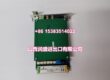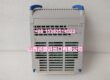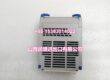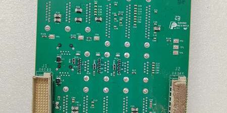
Component Snapshot At-a-Glance
- Model: 810-800082-043
- Alt. P/N: No factory cross-reference part number; no uncoated base variant
- Product Series: LAM Centura / Versys Metal / Sym3 Semiconductor Plasma Etch & Deposition Tools
- Hardware Type: VME64X I/O junction & signal distribution printed circuit board
- Key Feature: Multi-D-Sub field signal ports + dual 10/100 Ethernet, full factory conformal coating
- Primary Field Use: Route chamber edge detector, mass flow, RF power, and valve interlock signals between VME CPU and wafer processing chambers
Hard-Numbers: Technical Specifications
- Protocol Support: Modbus TCP, LAM proprietary tool Ethernet, VME backplane parallel bus
- Port Count: 2×RJ45 Ethernet, 18×DB9/DB25 D-Sub field signal connectors, VME64X rear edge connector
- Baud/Data Rate: Ethernet 10/100 Mbps auto-negotiate; VME bus 32-bit 40 MB/s throughput
- Operating Temperature: 10 °C to +45 °C (strict non-condensing fab environment; derate above 40 °C)
- Storage Temperature: -40 °C to +85 °C
- Isolation Rating: 1000 VAC galvanic isolation between field sensor wiring and VME backplane circuits
- Power Draw: Typical 7.2 W, max 9.5 W; 24 VDC nominal rack supply (21.6–26.4 VDC operating window)
- Mount Format: Standard 6U VME rack slot, vertical forced air cooling required
- PCB Coating: Full acrylic conformal coating to resist chemical vapors and fab humidity
- Ingress Protection: IP20, restricted to filtered cleanroom control cabinets only
- Signal Channels: 32 differential analog inputs, 64 discrete digital I/O paths multiplexed across D-Sub ports
- Calibration Requirement: Annual calibration via LAM CalibrateHV software for analog signal offset trim
The Real-World Problem It Solves
Discrete breakout terminal strips consume multiple VME rack slots and add dozens of intermediate wiring junctions; loose pins or unfiltered wiring create plasma process drift, inconsistent etch depth, and massive wafer scrap losses. Uncoated generic VME boards corrode quickly from fluorine and solvent vapors inside etch tool cabinets, triggering intermittent sensor dropout faults that force full chamber pump-down cycles to resolve. Single-Ethernet legacy junction boards create a single point of failure that halts all wafer transfer sequences.
Where you’ll typically find it:
- 300mm Centura dielectric etch tool main VME control racks for chamber edge detection and RF bias monitoring
- Versys metal physical vapor deposition (PVD) cabinets routing mass flow controller and gate valve interlock signals
- Sym3 multi-chamber wafer processing platforms handling robotic wafer position sensor feedback
Bottom-line value statement: Consolidated multi-signal junction design, dual redundant Ethernet, and vapor-resistant conformal coating cut rack slot usage, wiring fault points, and unplanned chamber downtime during high-volume wafer production runs.
Hardware Architecture & Under-the-Hood Logic
This board runs no standalone microprocessor; all signal processing and logic execution resides on the tool’s VME master CPU. Isolated analog front-end filters block high-frequency RF plasma noise from corrupting low-level edge detector signals. It plugs directly into the tool’s VME64X backplane via a rear gold-plated edge connector.
- 24 VDC VME rack power feeds isolated linear regulation circuits for analog sensor excitation and Ethernet transceivers
- All field D-Sub ports route discrete digital valve interlock and differential analog edge detector signals to on-board RC noise filter banks
- Galvanic isolation barriers separate every field signal group from the high-speed VME backplane bus to eliminate ground loop offsets
- Dual RJ45 Ethernet ports carry bidirectional process telemetry, fault logs, and recipe download data to the fab host MES network
- VME backplane edge connector multiplexes all conditioned analog/digital signals to the tool’s main CPU for recipe execution and fault limit comparison
- Front-panel bi-color LED indicators display VME bus activity, Ethernet link status, and per-port field signal open/short faults for rapid visual troubleshooting
Field Service Pitfalls: What Rookies Get Wrong
Skipping Compressed Air Filter Cleaning Before Module Replacement
New technicians swap this VME board without blowing accumulated fluorine dust from rack air intake vents. Trapped chemical residue coats the new PCB within weeks, creating intermittent high-impedance signal paths and drifting edge detector readings.
- Field Rule: Blow rack filter and card cage with dry <50 PSI nitrogen before every VME card swap; inspect conformal coating for discoloration post-cleaning.
Unshielded D-Sub Cable Runs Parallel With RF Generator Power Harnesses
Junior engineers route unshielded multi-pin signal cables alongside 13.56 MHz RF power wiring. Plasma switching noise injects offset into edge detector analog signals, generating false wafer edge misread faults and aborted process recipes.
- Quick Fix: Separate all D-Sub field cables from RF power runs by minimum 40 cm; install fully shielded DB hoods with single-point cabinet shield grounding.
Mismatched VME Backplane Firmware After PCB Replacement
Field crews install a replacement 810-800082-043 card without matching the VME CPU firmware revision. Ethernet handshakes fail entirely, and all chamber sensor tags go offline in the tool HMI.
- Field Rule: Cross-check VME controller firmware build against LAM tool spec sheet; run full hardware tree rescan and signal calibration trim post-card installation before wafer processing resumes.
Commercial Availability & Pricing Note
Please note: The listed price is for reference only and is not binding. Final pricing and terms are subject to negotiation based on current market conditions and availability.