Description
Detailed Parameter Table
| Parameter Name | Parameter Value |
| Product model | 810-069751-114 |
| Manufacturer | LAM Research |
| Product category | Plasma Impedance Matching Module (for Semiconductor Etching/Deposition Systems) |
| Operating Frequency Range | 400 kHz to 13.56 MHz (configurable via software) |
| Input Power Range | 100 W to 5000 W (RF power, continuous wave) |
| Impedance Matching Range | 5 Ω to 500 Ω (load impedance); 50 Ω (source impedance, fixed) |
| Matching Speed | <50 μs (full impedance adjustment, step response) |
| Interface Type | Ethernet (10/100/1000Base-T); RS-485; 2x 24-pin terminal blocks (power/signals); 1x USB-C (configuration); 1x RF input/output port (N-type connector) |
| Communication Protocol | Modbus TCP/IP, EtherNet/IP, LAM Proprietary PlasmaLink™ v3.0 |
| Operating Temperature Range | 15°C to 45°C (non-condensing) |
| Relative Humidity Tolerance | 10% to 80% RH (non-condensing, no moisture ingress) |
| Physical Dimensions (W×H×D) | 280mm × 320mm × 160mm (excluding connectors/RF ports) |
| Installation Method | 19-inch rack mounting (4U height); panel mounting (with RF-shielded brackets) |
| Certifications | CE, UL 61010-1, SEMI S2/S8/S14 (semiconductor safety/EMC/RF standards) |
| Power Consumption | 24V DC (logic): 1.2A typical; 48V DC (actuation): 3.5A max (matching network) |
| RF Efficiency | ≥95% (at 13.56 MHz, full load) |
| Monitoring Metrics | Real-time RF power (forward/reflected), impedance, VSWR (Voltage Standing Wave Ratio), temperature |
| Protection Features | Over-power (5500 W max), high VSWR (>2.5:1 shutdown), over-temperature (70°C) |
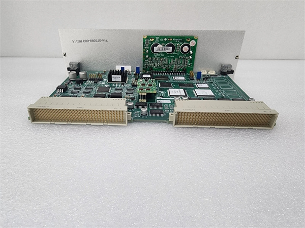
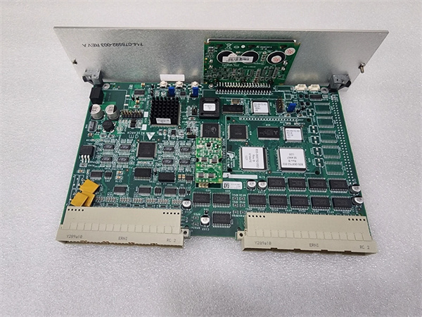
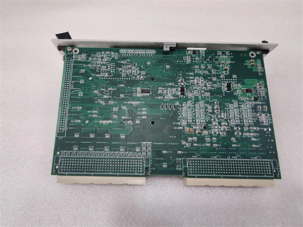
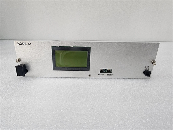
LAM 810-069751-114
Product Introduction
The 810-069751-114 is a high-performance plasma impedance matching module developed by LAM Research, a global leader in semiconductor manufacturing equipment. Explicitly engineered for integration into LAM’s flagship plasma-based platforms—including Centura® AdvantEdge™ Etch, Sym3® Plasma Enhanced CVD (PECVD), and Versys® Metal Etch systems—this module serves as the “RF power optimizer” for semiconductor processing, ensuring efficient, stable power transfer to plasma chambers.
As a flagship model in LAM’s Plasma Control Series, the 810-069751-114 is optimized for 3nm and 2nm process nodes, where plasma stability (governed by impedance matching) is non-negotiable for minimizing etch defects or thin-film non-uniformity. Its core function is to dynamically adjust an internal RF matching network to align the chamber’s load impedance (5–500 Ω) with the RF generator’s fixed source impedance (50 Ω), eliminating reflected power and maximizing energy delivered to the plasma. In automation systems, the 810-069751-114 acts as a critical link between RF generators and process chambers—synchronizing impedance adjustments with other subsystems like the 839-101870-002 pressure control module and 739-090783-001 gas flow module to maintain consistent plasma chemistry.
Core Advantages and Technical Highlights
Ultra-Fast Impedance Matching: The 810-069751-114 achieves full impedance adjustment in <50 μs—up to 4x faster than legacy matching modules (typically 200–300 μs)—a game-changer for 2nm/3nm processes where plasma conditions shift rapidly (e.g., during etch recipe transitions). This speed is enabled by a digital matching network with piezoelectric actuators (vs. mechanical motors in older models) and a proprietary adaptive algorithm that predicts impedance changes based on real-time process data. For example, when the 839-101870-002 adjusts chamber pressure, the 810-069751-114 pre-emptively tweaks impedance to offset pressure-induced plasma shifts, keeping VSWR <1.2:1 (a threshold for stable plasma).
Broad Frequency and Power Compatibility: Unlike single-frequency matching modules, the 810-069751-114 supports a 400 kHz–13.56 MHz range—covering the full spectrum of RF frequencies used in semiconductor processing (e.g., 400 kHz for deep silicon etching, 13.56 MHz for PECVD). It also handles 100–5000 W of RF power, making it compatible with both low-power R&D tools and high-volume production systems. Its ≥95% RF efficiency minimizes energy waste and heat generation, reducing fab operational costs and extending the module’s mean time between failures (MTBF) to over 150,000 hours.
Comprehensive RF Monitoring and Diagnostics: The 810-069751-114 provides granular real-time data on forward/reflected RF power, load impedance, VSWR, and internal temperature—all accessible via Ethernet or USB-C. It logs these metrics for up to 90 days, enabling engineers to correlate impedance drift with process defects (e.g., high reflected power linked to etch non-uniformity). The module also includes proactive alerts: if VSWR exceeds 2.0:1 (a pre-shutdown warning), it sends a signal to the main controller to adjust gas flow or pressure via the 739-090783-001 or 839-101870-002—preventing costly RF generator damage or wafer scrappage.
Semiconductor-Grade RF Shielding and Durability: Built to SEMI S2/S8/S14 standards, the 810-069751-114 features a double-layer RF-shielded housing (attenuating stray RF emissions by >60 dB) to avoid interfering with sensitive tools like the 715-015169-011 optical sensor module. Its internal components are coated with a ceramic-fluoropolymer composite to resist corrosion from plasma byproducts (e.g., fluorides, chlorides), while a liquid-cooled heat sink maintains optimal operating temperature—critical for preserving the precision of the matching network’s piezoelectric actuators.
Typical Application Scenarios
The 810-069751-114 is indispensable in fabs for plasma-critical operations, with two high-impact use cases: deep silicon etching for 3D NAND and PECVD for 2nm logic thin films.
In deep silicon etching (e.g., LAM’s Centura® AdvantEdge™ Etch for 3D NAND), the 810-069751-114 optimizes RF power transfer at 400 kHz—an ultra-low frequency that enables deep, high-aspect-ratio (HAR) trench formation (aspect ratios >100:1). During etching, the chamber’s load impedance fluctuates as trenches deepen (due to changing plasma density), but the 810-069751-114 adjusts the matching network in <50 μs to keep reflected power <5% of forward power. This stability ensures uniform trench depth across the wafer, reducing 3D NAND cell-to-cell capacitance variation by 30% compared to legacy modules. Fabs using the 810-069751-114 also report a 25% reduction in etch time, as higher RF efficiency delivers more energy to the plasma.
In PECVD for 2nm logic (e.g., Sym3® PECVD), the 810-069751-114 operates at 13.56 MHz to maintain stable plasma for depositing ultra-thin (5–10nm) dielectric layers. It synchronizes impedance adjustments with the 739-090783-001 gas flow module: when the module increases precursor flow (e.g., TEOS for SiO₂), the 810-069751-114 tweaks impedance to offset the resulting plasma density change. This coordination ensures film thickness uniformity of ±2% across 300mm wafers—critical for 2nm logic devices, where dielectric layer variations cause signal delay or leakage. The module’s VSWR protection also prevents RF-induced damage to the PECVD chamber’s electrode, a component that costs tens of thousands of dollars to replace.
LAM 810-069751-114
Related Model Recommendations
LAM 810-069751-115: An upgraded variant of the 810-069751-114 with extended power range (100 W–8000 W) and dual RF ports—designed for high-power applications like metal etching for advanced packaging.
LAM 810-069751-113: A compact variant of the 810-069751-114 (3U rack height, 400 kHz–6 MHz range) with reduced power capacity (100 W–3000 W)—ideal for R&D labs or small-scale PECVD tools.
LAM 810-069752-114: A redundant impedance matching module that pairs with the 810-069751-114 for fault-tolerant fabs (e.g., high-yield memory production), automatically taking over if the primary module fails to prevent plasma shutdown.
LAM 810-069750-114: A legacy replacement for LAM’s pre-2020 matching modules (e.g., 810-069748-001), fully compatible with the 810-069751-114’s mounting, power, and protocol support.
LAM 810-069751-116: A high-temperature variant of the 810-069751-114 (operating range: 10°C–55°C) with enhanced liquid cooling—designed for use near high-heat tools like MOCVD systems.
LAM 810-069753-114: An RF monitoring accessory module that adds real-time spectrum analysis to the 810-069751-114, detecting harmonic distortion and RF noise that could disrupt plasma stability.
LAM 810-069751-117: A low-frequency-optimized variant of the 810-069751-114 (10 kHz–400 kHz) for specialized processes like inductively coupled plasma (ICP) etching for MEMS.
LAM 810-069754-114: A calibration accessory module that provides NIST-traceable RF power/impedance references for the 810-069751-114, simplifying on-site calibration and eliminating lab send-in requirements.
Installation, Commissioning and Maintenance Instructions
Installation Preparation: Before installing the 810-069751-114, ensure the 19-inch rack is RF-shielded (per SEMI S14 standards) and ambient temperature is 15–45°C. Required tools include a torque wrench (3.0 N·m for rack mounting), RF power meter (to verify generator output), ESD-safe gloves/wristbands, and a laptop (for USB-C configuration). Safety precautions: Disconnect RF generator power and DC power to the module before wiring; use RG-214 coaxial cables (rated for 13.56 MHz, 5000 W) for RF connections to minimize signal loss; torque N-type connectors to 1.5 N·m (over-tightening damages RF ports); confirm the module’s ground connection (≥8AWG wire) is secure to prevent RF leakage. Avoid mounting near optical sensors (e.g., 715-015169-011) or digital I/O modules (e.g., 810-007215-002) to prevent RF interference.
Maintenance Suggestions: For daily maintenance, check the 810-069751-114’s front-panel LED indicators (green = normal, amber = high VSWR, red = fault) and review RF metrics via PlasmaLink™ software. Every 3 months, clean the liquid-cooled heat sink’s inlet/outlet filters (use deionized water) to prevent clogging—overheating degrades piezoelectric actuator performance. Every 12 months, perform a calibration check using the LAM 810-069754-114 accessory to verify impedance matching accuracy and RF efficiency; replace coaxial cables if VSWR exceeds 1.1:1 (indicates cable degradation). If a fault occurs (e.g., over-temperature), first shut down the RF generator, inspect cooling lines for leaks, and use the module’s diagnostic log to identify the root cause—never open the RF-shielded housing, as internal components carry high voltages and require factory servicing.
Service and Guarantee Commitment
The 810-069751-114 comes with a 48-month manufacturer’s warranty from LAM Research, covering defects in materials, workmanship, and RF performance under normal use (per SEMI S2/S8/S14 standards). If the module fails within the warranty period, LAM provides a “rapid swap” service—delivering a pre-calibrated replacement unit within 24 hours (for Priority Service customers) to minimize plasma tool downtime, with no cost for repair, shipping, or reconfiguration.
LAM offers 24/7 technical support for the 810-069751-114, including access to RF engineering specialists via phone/email, remote diagnostics (via secure Ethernet), and on-site troubleshooting (available within 48 hours globally). The module includes free access to LAM’s PlasmaSuite™ software (for configuration, calibration, and firmware updates) for 5 years post-purchase, ensuring compatibility with future RF generator technologies and 2nm+ process nodes.
To enhance reliability, LAM offers a Plasma Impedance Care Program for the 810-069751-114, which includes scheduled on-site RF performance checks, proactive cooling system maintenance, and annual NIST-traceable calibration—tailored to the fab’s production schedule. This commitment reflects LAM’s confidence in the 810-069751-114’s durability and its dedication to supporting customers’ plasma-critical semiconductor manufacturing operations.