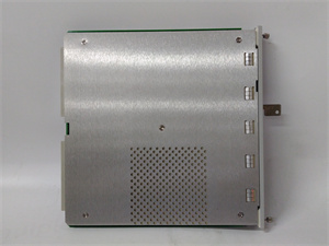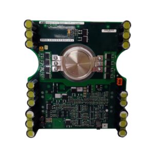
Description
Detailed Parameter Table
| Parameter Name | Parameter Value |
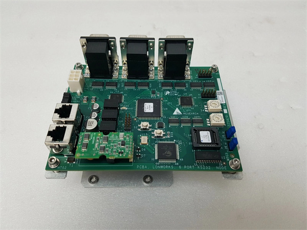
| Product model | 715-015169-011 |
| Manufacturer | LAM Research |
| Product category | Precision Optical Sensor Interface Module (for Semiconductor Processing Systems) |
| Sensor Compatibility | Wafer alignment sensors (CCD/CMOS), film thickness monitors (ellipsometers/spectrometers), particle detectors |
| Input Channels | 4x analog optical inputs (0–10V DC, 24-bit resolution); 2x digital optical inputs (TTL level) |
| Output Signals | 2x analog processed outputs (0–5V DC, 16-bit); 4x digital trigger outputs (24V DC, sinking) |
| Signal Sampling Rate | 1MSPS (analog inputs); 10MSPS (digital inputs) |
| Signal-to-Noise Ratio (SNR) | ≥85dB (analog inputs, at full scale) |
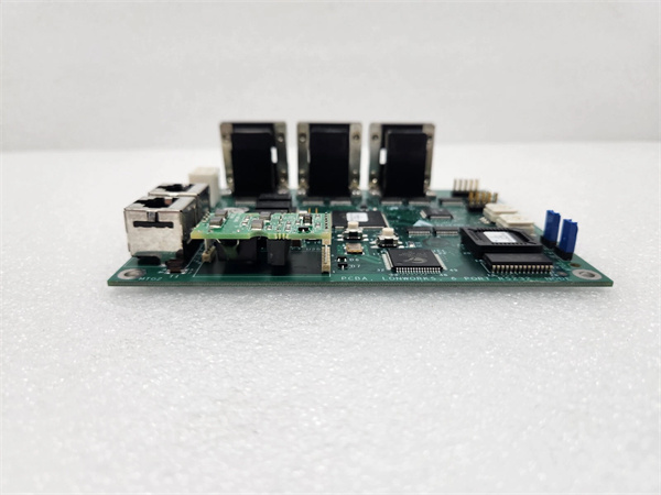
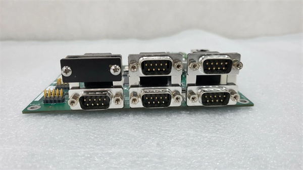
| Interface Type | Ethernet (10/100/1000Base-T); RS-485; 2x 32-pin terminal blocks (power/sensor signals); 1x USB-C (configuration); 1x SFP+ (for high-speed optical data) |
| Communication Protocol | EtherNet/IP, Modbus TCP/IP, LAM Proprietary OptiLink™ |
| Operating Temperature Range | 10°C to 40°C (non-condensing) |
| Relative Humidity Tolerance | 15% to 75% RH (non-condensing, no moisture ingress) |
| Physical Dimensions (W×H×D) | 180mm × 220mm × 90mm (excluding connectors/terminal blocks) |
| Installation Method | DIN rail mounting (35mm standard); panel mounting (with optional low-profile brackets) |
| Certifications | CE, UL 61010-1, SEMI S2/S8/S14 (semiconductor safety/EMC standards) |
| Power Consumption | 24V DC, 0.9A typical; 1.5A maximum (when all channels are active) |
| Signal Filtering | Configurable low-pass filter (1Hz–10kHz); adaptive noise cancellation |
| Calibration Support | NIST-traceable internal calibration reference; software-guided calibration wizard |
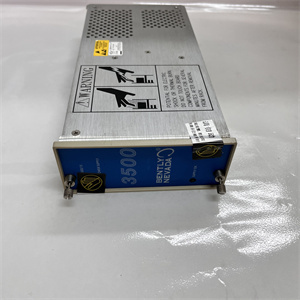
LAM 810-225420-002
Product Introduction
The 715-015169-011 is a high-performance precision optical sensor interface module developed by LAM Research, a global leader in semiconductor manufacturing equipment. Specifically engineered to integrate with LAM’s flagship processing platforms—including Centura® Etch, Sym3® CVD, and Versys® Metal Deposition systems—this module serves as the “optical signal translator” for connecting sensitive optical sensors to the central control system.
As a core model in LAM’s Optical Control Series, the 715-015169-011 is optimized for advanced semiconductor process nodes (down to 3nm), where sub-micron alignment accuracy and nanoscale film thickness measurement are non-negotiable for device performance. Its core function is to receive, amplify, and process raw signals from optical sensors (e.g., wafer alignment CCDs, ellipsometers), then transmit calibrated, low-noise data to the main controller. In automation systems, the 715-015169-011 acts as a critical link between optical hardware and subsystems like the 810-013872-105 motion control module—translating alignment sensor data into precise stage adjustments, ensuring wafers are positioned within ±0.1μm of the target.
Core Advantages and Technical Highlights
Ultra-High Signal Integrity and Low Noise: The 715-015169-011 delivers exceptional signal quality with an SNR of ≥85dB and 24-bit analog resolution—far exceeding basic optical interfaces (typically 16-bit, 60dB SNR). This is achieved through a combination of low-noise preamplifiers, adaptive noise cancellation (which suppresses EMI from nearby tools like vacuum pumps), and configurable low-pass filters. For 3nm wafer alignment, this means the module can detect sub-micron shifts in sensor signals, enabling the 810-013872-105 motion module to make adjustments as small as 0.05μm—critical for preventing overlay errors in multi-layer patterning.
Multi-Sensor Versatility: Unlike single-purpose optical interfaces, the 715-015169-011 supports multiple optical sensor types: wafer alignment sensors (CCD/CMOS), film thickness monitors (ellipsometers), and particle detectors. Each of its 4 analog inputs can be independently configured (gain, filter settings) via software to match the sensor’s output characteristics—eliminating the need for separate interface modules. For example, it can simultaneously process signals from a CCD alignment sensor (0–2V DC) and an ellipsometer (0–10V DC), then send calibrated data to the controller for real-time alignment and film quality checks.
Rapid Signal Processing and Sync: With a 1MSPS analog sampling rate and 10MSPS digital sampling rate, the 715-015169-011 ensures near-instantaneous signal processing—critical for high-throughput production lines where wafer alignment must be completed in <1 second per wafer. It also supports PTP (Precision Time Protocol) v2.1, enabling synchronization (±50ns accuracy) with other modules like the 810-225420-002 DAQ module. This sync ensures that optical data (e.g., film thickness at position X) is time-stamped to match mechanical data (e.g., stage position at X), simplifying root-cause analysis of process defects.
Semiconductor-Grade Reliability: Built to comply with SEMI S2/S8/S14 standards, the 715-015169-011 features a corrosion-resistant polymer housing (to withstand low-level process gas leaks, e.g., ammonia, fluorine) and gold-plated terminal blocks (for stable signal connections). Its internal components are rated for long-term stability, with a mean time between failures (MTBF) exceeding 180,000 hours—far longer than consumer-grade optical interfaces. The module also includes reverse-polarity protection on sensor inputs, preventing damage from accidental wiring errors (a common issue during maintenance).
Typical Application Scenarios
The 715-015169-011 is indispensable in semiconductor fabs for optical-critical operations, with two high-impact use cases: wafer alignment for advanced patterning and real-time film thickness monitoring in CVD processes.
In wafer alignment (e.g., LAM’s Centura® Etch for 3nm logic devices), the 715-015169-011 processes signals from a CCD alignment sensor mounted above the wafer stage. The sensor captures images of alignment marks on the wafer, converting them into analog voltage signals (0–5V DC) that the 715-015169-011 amplifies and filters to remove noise. The module then transmits calibrated position data to the 810-013872-105 motion control module, which adjusts the stage to align the wafer with the etch chamber’s plasma source—all within 800ms. This speed and accuracy reduce overlay errors (a leading cause of device failure) by up to 30% compared to legacy alignment systems.
In real-time film thickness monitoring (e.g., Sym3® CVD for 3D NAND dielectric layers), the 715-015169-011 connects to an ellipsometer that measures film thickness via light reflection. The ellipsometer outputs raw analog signals (0–10V DC) that the 715-015169-011 processes using a built-in ellipsometry algorithm, converting them into calibrated thickness values (e.g., 5.2nm ±0.1nm). The module sends this data to the central controller, which adjusts CVD parameters (e.g., precursor flow via the 739-090783-001 gas module) if thickness deviates from the target. Fabs using the 715-015169-011 report a 22% reduction in film thickness variation, directly improving 3D NAND memory cell performance.
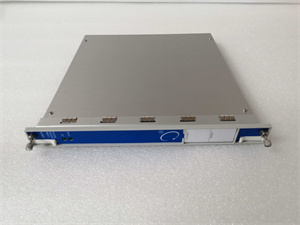
LAM 810-225420-002
Related Model Recommendations
LAM 715-015169-012: An upgraded variant of the 715-015169-011 with 8 analog inputs (vs. 4) and dual SFP+ ports (for redundant high-speed optical data), designed for large-scale tools (e.g., 8-chamber etch systems with multiple alignment sensors).
LAM 715-015169-010: A compact variant of the 715-015169-011 (2 analog inputs, 1 digital input) with reduced power consumption (0.6A typical), ideal for R&D labs or small-scale tools (e.g., single-chamber ALD systems).
LAM 715-015170-011: A redundant optical interface module that pairs with the 715-015169-011 for fault-tolerant systems (e.g., high-yield memory fabs), automatically taking over signal processing if the primary module fails to prevent alignment errors.
LAM 715-015168-011: A legacy replacement for LAM’s pre-2020 optical modules (e.g., 715-015165-001), fully compatible with the 715-015169-011’s mounting, power, and protocol support.
LAM 715-015169-013: A high-temperature variant of the 715-015169-011 (operating range: 5°C to 50°C) with enhanced thermal shielding, designed for use near high-heat tools (e.g., MOCVD systems for compound semiconductors).
LAM 715-015171-011: An optical calibration accessory module that provides NIST-traceable light sources for the 715-015169-011, simplifying on-site sensor calibration and eliminating the need for external calibration tools.
LAM 715-015169-014: A wireless-enabled variant of the 715-015169-011 (Wi-Fi 6, Bluetooth 5.2), enabling remote monitoring of optical sensor data for hard-to-access tools (e.g., ceiling-mounted wafer inspection systems).
LAM 715-015172-011: A particle detection-focused variant of the 715-015169-011 with specialized signal processing for particle sensors, optimized for cleanroom monitoring in 3nm process fabs.
Installation, Commissioning and Maintenance Instructions
Installation Preparation: Before installing the 715-015169-011, ensure the DIN rail/panel is clean (free of particulate matter) and the ambient temperature is within 10–40°C. Required tools include a torque screwdriver (0.5 N·m for DIN rail mounting), multimeter (to verify 24V DC power), ESD-safe gloves/wristbands, and a laptop (for USB-C configuration). Safety precautions: Disconnect power to the host system before wiring; use shielded, twisted-pair cables for sensor inputs (to minimize EMI, critical for signal integrity); and confirm the module’s ground connection (≥12AWG wire) is secure to prevent ESD damage. Avoid mounting near high-voltage components (e.g., plasma power supplies) or sources of vibration (e.g., pumps) to prevent signal noise.
Maintenance Suggestions: For daily maintenance, check the 715-015169-011’s front-panel LED indicators (green = normal, amber = signal warning, red = critical fault) and verify sensor signal strength via the OptiLink™ software. Every 6 months, perform a software-guided calibration using the module’s internal reference (or LAM 715-015171-011 accessory) to maintain signal accuracy—this is especially critical for ellipsometer signals, where drift can cause film thickness measurement errors. Every 12 months, inspect terminal blocks for corrosion (common in fab environments) and replace shielded cables if noise levels exceed 10mV (measured via the module’s diagnostic tool). If a fault occurs (e.g., low SNR on an input channel), first check sensor wiring for loose connections, then use the module’s built-in noise analysis tool to identify EMI sources—relocate the module or add additional shielding if needed.
Service and Guarantee Commitment
The 715-015169-011 comes with a 36-month manufacturer’s warranty from LAM Research, covering defects in materials, workmanship, and optical signal processing performance under normal use (per SEMI S2/S8 operating conditions). If the module fails within the warranty period, LAM provides a “rapid swap” service—delivering a pre-calibrated replacement unit within 48 hours (for Priority Service customers) to minimize tool downtime, with no cost for repair, shipping, or reconfiguration.
LAM offers end-to-end technical support for the 715-015169-011, including 24/7 access to optical control specialists via phone/email, remote diagnostics (via secure Ethernet), and on-site troubleshooting (available within 72 hours for global fabs). The module also includes free access to LAM’s OptiSuite™ software (for configuration, calibration, and firmware updates) for 5 years post-purchase, ensuring compatibility with new optical sensor technologies (e.g., next-gen CMOS alignment sensors for 2nm nodes).
To enhance reliability, LAM offers an Optical Interface Care Program for the 715-015169-011, which includes scheduled on-site inspections, proactive cable replacement, and annual NIST-traceable calibration—tailored to the fab’s production schedule. This commitment reflects LAM’s confidence in the 715-015169-011’s quality and its dedication to supporting customers’ precision-driven semiconductor manufacturing operations.