Description
Hard-Numbers: Technical Specifications
- DAC Resolution: 16 bits
- Analog Bandwidth: 80 MHz (-3 dB)
- DAC Update Rate: 800 MS/s
- Maximum Arbitrary Waveform Rate: 400 MS/s (digital filter enabled), 250 MS/s (digital filter disabled)
- Standard Function Range: 0 µHz to 80 MHz
- Onboard Memory: 512 MB (785117-01, 785118-01)
- Channel Count: 1 (785117-01) or 2 (785118-01) independent generation engines
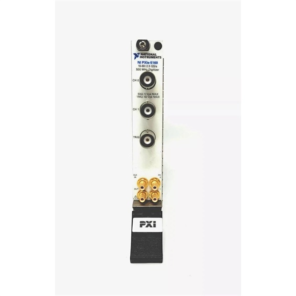
- Output Type: Referenced single-ended
- Connector Type: SMA
- Output Impedance: 50 Ω
- Load Impedance: Compensated for user-specified impedances
- Output Coupling: DC (ground referenced)
- Amplitude Range: 0.00775 Vpk-pk to 12 Vpk-pk (50 Ω load); 0.0155 Vpk-pk to 24 Vpk-pk (open load)
- Offset Range: ±50% of Amplitude Range (Vpk-pk)
- DC Accuracy (within ±5°C of self-calibration): ±0.35% of Amplitude Range ± 0.35% of Offset Requested ± 500 µV
- AC Amplitude Accuracy (within ±5°C of self-calibration): ±1.0% ± 1 mVpk-pk
- Passband Flatness: ±0.4 dB (1-80 MHz, <2.75 Vpk-pk)
- Rise Time: 4.5 ns (<2.75 Vpk-pk), 5.4 ns (>2.75 Vpk-pk)
- Spurious-Free Dynamic Range (SFDR) : -92 dB (typical)
- Phase Noise: -100 dBc/Hz @ 10 Hz offset, -120 dBc/Hz @ 1 kHz offset, -130 dBc/Hz @ 10 kHz offset
- Integrated System Jitter: 435 fs
- Sample Clock Rate: 800 MHz
- Timebase Accuracy: Initial calibrated accuracy 1.5 ppm (warranted), time drift 1 ppm/year (warranted)
- Reference Clock: Internal PXIe_CLK100 (backplane), 100 MHz (<±25 ppm)
- Channel-to-Channel Skew: ±110 ps (<2.75 Vpk-pk), ±275 ps (>2.75 Vpk-pk)
- Digital Filter: On/Off (removes frequency images when enabled)
- Minimum Sample Rate: 5.6 µS/s (digital filter enabled), 10 S/s (digital filter disabled)
- Self-Calibration: ~2 minutes
- Warm-Up Time: 15 minutes
- Operating Temperature: 0°C to 55°C
- Storage Temperature: -40°C to 71°C
- Relative Humidity: 10% to 90% noncondensing (operating), 5% to 95% noncondensing (storage)
- Power Consumption: +3.3 V @ 2.3 A, +12 V @ 1.8 A; total 29 W
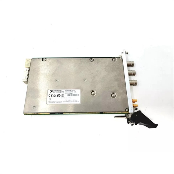
- Dimensions: 3U one-slot PXI Express module, 21.6 cm × 2.0 cm × 13.0 cm (8.5 in × 0.8 in × 5.1 in)
- Weight: 369 g (13.0 oz, 1 CH); 376 g (13.3 oz, 2 CH)
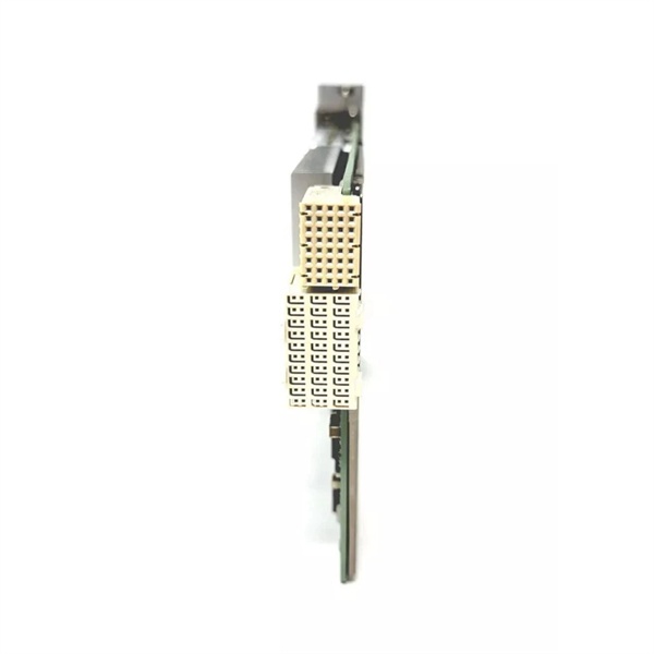
- Bus Interface: PXI Express Gen 1 x4
- Slot Compatibility: PXI Express or hybrid
- Calibration Interval: 2 years
- Compliance: IEC 61010-1, EN 61326-1, FCC Part 15B Class A
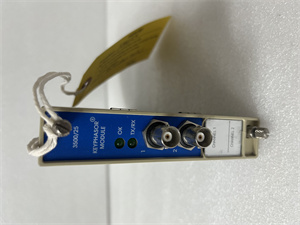
NI PXIe-5172
The Real-World Problem It Solves
Traditional arbitrary waveform generators with fixed update rates compromise signal purity when reducing sample rate or generate frequency images that corrupt output spectra. The PXIe-5433 delivers 800 MS/s DAC update rate with fractional resampling, maintaining -92 dBc SFDR across user sample rates while eliminating frequency images through digital filtering. Independent generation engines per channel enable truly multi-channel synchronized stimulus without shared resource conflicts, reducing test time in automated semiconductor validation and automotive electronics testing.
Where you’ll typically find it:
- Semiconductor validation stimulating DUTs with complex multi-tone signals requiring precise phase relationships and spectral purity
- Automotive ECU testing simulating sensor and communication signals with synchronized multi-channel output for functional validation
- Aerospace/defense applications generating radar and IF/RF signals with high fidelity and sub-nanosecond synchronization with other PXI modules
Bottom line: This AWG replaces multiple function generators and eliminates frequency image artifacts through fractional resampling and digital filtering, delivering independent per-channel generation engines with 800 MS/s update rate for synchronized multi-channel stimulus in automated test systems.
Hardware Architecture & Under-the-Hood Logic
The PXIe-5433 is built on a fractional resampling architecture with independent per-channel generation engines, featuring 16-bit DACs updating at 800 MS/s and deep onboard memory. Each channel has its own generation engine, enabling independent configuration for triggers, markers, and waveform scripts—channels do not share execution resources. The FPGA implements fractional resampling to up-sample user-defined arbitrary waveforms to 800 MS/s, maintaining consistent dynamic range and jitter performance across sample rates. Digital filtering removes frequency images from arbitrary waveforms when enabled, improving spectral purity at the cost of reduced slew rate. The PXI Express Gen 1 x4 interface supports waveform streaming, and the module supports NI-TClk for multi-instrument synchronization. A precision TCXO provides 1.5 ppm initial accuracy with 1 ppm/year drift.
- Waveform data (standard functions or arbitrary waveforms) uploaded from host to onboard memory (512 MB) → FPGA fractional resampling engine up-samples user waveforms to 800 MS/s DAC update rate
- Generation engine per channel: Each channel operates independently with its own trigger, marker, and script configuration → No shared execution resources between channels (except reference clock and external PFI trigger input)
- Digital filter stage: Removes frequency images at multiples of programmed sample rate when enabled → Improves spectral purity (-92 dBc SFDR typical); disabled mode includes high-frequency content for faster slew rates
- 16-bit DAC stage: Converts up-sampled digital data to analog at 800 MS/s → 0.00775 Vpk-pk to 12 Vpk-pk into 50 Ω load, 0.0155 Vpk-pk to 24 Vpk-pk into high-impedance load
- Output amplifier: Provides signal amplification and offset (±50% of amplitude range) → Output impedance 50 Ω, DC-coupled (ground referenced), SMA connector
- Clock distribution: Internal TCXO (1.5 ppm initial, 1 ppm/year drift) or PXIe_CLK100 backplane reference (±25 ppm) → 800 MHz sample clock distributed to DAC with 435 fs integrated jitter
- Synchronization: NI-TClk API aligns sample clocks of PXI modules using shared reference clock and triggers routed through PXI chassis backplane → Channel-to-channel skew ±110 ps (<2.75 Vpk-pk), ±275 ps (>2.75 Vpk-pk)
- Trigger system: Rising edge triggers only (PXIe-54×3 standardization) → Sources include PXI_Trig backplane, PFI lines, software triggers
- Memory management: Deep onboard memory (512 MB) stores waveforms and sequences → Frequency List mode supports up to 1024 steps for fast frequency hopping/sweeping
- Calibration: Self-calibration uses onboard reference to correct DC gain and offset (~2 minutes) → External calibration calibrates TCXO, voltage reference, and DC gain/offset (2-year interval)

NI PXIe-5172
Field Service Pitfalls: What Rookies Get Wrong
Connecting Multiple PXIe-5433 Outputs Together
Technicians assume multiple PXIe-5433 outputs can be directly connected for power summation or signal combining without damage. While the datasheet states “No damage occurs if the analog output channels are shorted to ground indefinitely,” connecting multiple outputs together can cause unpredictable signal levels and potential current conflicts in the 50 Ω output stage.
- Field Rule: Never directly connect AWG outputs together unless using external resistive combiners or summing networks designed for signal addition. Verify each output is terminated into its proper load impedance (50 Ω or user-specified). If summing signals is required, use external resistive combiners with appropriate isolation. Remember: 50 Ω outputs are designed to drive 50 Ω loads, not other 50 Ω sources.
Ignoring Passband Flatness Degradation Above 45°C
Engineers assume the ±0.4 dB passband flatness specification applies across the full 0-55°C operating range. Above 45°C ambient temperature with sine frequencies 40 MHz or higher, add ±0.015 dB/°C to the passband flatness specification. At 55°C, this adds ±0.15 dB degradation, causing amplitude errors in high-frequency calibration applications.
- Quick Fix: Monitor chassis inlet temperature. If ambient exceeds 45°C, account for ±0.015 dB/°C additional passband flatness degradation for signals 40 MHz and above. For critical calibration applications, maintain ambient below 45°C using external cooling or relocate the test rack. Remember: passband flatness is warranted at 0-55°C, but the additional temperature coefficient applies above 45°C for high-frequency signals.
Enabling Flatness Correction with Digital Gain Changes
Users attempt to change digital gain on-the-fly while flatness correction is enabled. When flatness correction is enabled, digital gain cannot be changed on-the-fly because flatness correction requires pre-computed digital correction coefficients.
- Field Rule: Disable flatness correction before changing digital gain, or pre-compute gain values and upload the corrected waveform. For applications requiring on-the-fly gain adjustment, disable flatness correction and accept reduced passband flatness. Remember: flatness correction improves sine wave amplitude accuracy across frequency but locks digital gain settings.
Forgetting Minimum On/Off Time Limits at High Frequencies
Rookies ignore minimum on-time and off-time specifications when generating square waves at high frequencies. At 80 MHz, the minimum on-time and off-time limit the duty cycle range—extreme duty cycles cannot be generated because the output amplifier cannot switch fast enough.
- Field Rule: Calculate minimum and maximum duty cycles using: Minimum Duty Cycle = (100% × Minimum On Time) ÷ Tperiod, Maximum Duty Cycle = 100% – Minimum Duty Cycle. At high frequencies, verify your required duty cycle falls within these limits. If not, reduce frequency or accept duty cycle distortion. Remember: minimum on-time is a hardware limit imposed by output amplifier slew rate.
Mixing Multi-Channel and Single-Channel Sessions Incorrectly
Users create a single multi-channel session for PXIe-5433 and attempt to write different waveforms to individual channels. PXIe-54×3 devices do not allow writing a waveform to a single channel when in multi-channel mode—both channels must be written with interleaved data.
- Field Rule: For independent waveforms per channel, create separate independent sessions for each channel. For multi-channel mode with different waveforms, write interleaved data for both channels. Remember: multi-channel mode treats both channels as a combined resource—independent waveforms require independent sessions or interleaved data.
Commercial Availability & Pricing Note
Please note: The listed price is for reference only and is not binding. Final pricing and terms are subject to negotiation based on current market conditions and availability.