Description
Hard-Numbers: Technical Specifications
- Resolution: 14-bit (16,384 levels)
- Analog Bandwidth: 100 MHz (-3 dB warranted, 99 MHz on 0.2 V range at 50 Ω; 98 MHz on 1 MΩ all ranges)
- Real-Time Sampling Rate: 250 MS/s (single-shot, all channels simultaneously sampled)
- Onboard Memory: 750 MB (784224-01, 784225-01) or 1.5 GB (784226-01)
- Data Streaming: 3.2 GB/s maximum (PXI Express Gen 2 x8)
- Channel Count: 4 (784224-01) or 8 (784225-01, 784226-01) simultaneously sampled channels
- Input Impedance: 50 Ω ±1.5% (typical) or 1 MΩ ±0.5% (typical, 16 pF ±1.2 pF input capacitance)
- Voltage Ranges: 0.2 Vpk-pk, 0.7 Vpk-pk, 1.4 Vpk-pk, 5 Vpk-pk (50 Ω and 1 MΩ)
- Maximum Input Overload: 50 Ω: peaks ≤10 V; 1 MΩ: peaks ≤42 V
- Spurious-Free Dynamic Range (SFDR) : -70 dBc to -80 dBc (depending on range, ≤30 MHz input)
- Total Harmonic Distortion (THD) : -74 dBc to -77 dBc (depending on range, ≤30 MHz input)
- Effective Number of Bits (ENOB) : 9.8 to 11.9 bits (depending on range and filter settings)
- Rise/Fall Time: 5.15 ns (50 Ω), 5.25 ns (1 MΩ)
- Trigger Types: Edge, hysteresis, window, digital, immediate, software
- Trigger Jitter: 15 ps RMS
- Trigger Accuracy: 0.75% FS (0.2 V range); 0.5% FS (0.7 V, 1.4 V, 5 V ranges)
- Sample Clock Jitter: 700 fs RMS
- Timebase Accuracy: ±25 ppm (phase-locked to onboard clock)
- External Sample Clock Range: 150 MHz to 250 MHz
- Bandwidth-Limiting Filters: 20 MHz, 40 MHz, 80 MHz (digital FIR filters)
- AC Coupling Cutoff (-3 dB) : 16.50 Hz
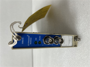
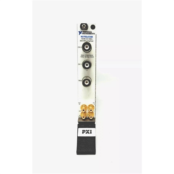
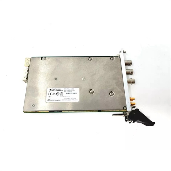
- Input Connectors: SMB (CH0-CH7), ground referenced
- FPGA: Xilinx Kintex-7 XC7K325T (4 CH models) or XC7K410T (8 CH models)
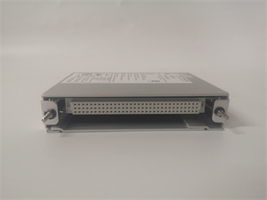
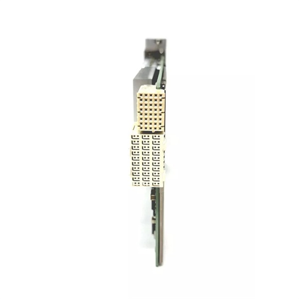
- Bus Interface: PXI Express Gen 2 x8
- Operating Temperature: 0°C to 45°C
- Storage Temperature: -40°C to 71°C
- Relative Humidity: 10% to 90% noncondensing
- Power Consumption: +12 V @ 13.75 W (typical), +3.3 V @ 6.5 W (typical); total ~20.25 W typical
- Dimensions: 3U one-slot PXI Express module, 18.5 cm × 2.0 cm × 13.0 cm (7.3 in × 0.8 in × 5.1 in)
- Weight: 449 g (15.8 oz, 4 CH); 461 g (16.3 oz, 8 CH)
- Calibration Interval: 2 years
- Compliance: IEC 61010-1, EN 61326-1, FCC Part 15B Class A
NI PXIe-5172
The Real-World Problem It Solves
High-channel-count test systems requiring simultaneous sampling across 4 or 8 channels at 250 MS/s with FPGA-based custom processing have traditionally required multiple instruments or expensive custom hardware. The PXIe-5172 delivers 4 or 8 simultaneously sampled channels with a user-programmable Kintex-7 FPGA in a single PXI slot, enabling custom acquisition, triggering, signal processing, and 3.2 GB/s streaming without sacrificing real-time performance.
Where you’ll typically find it:
- Automotive electronics testing capturing multiple sensor or ECU channels simultaneously with custom FPGA-based signal processing for real-time analysis
- Semiconductor test systems requiring high-channel-count parallel acquisition with custom triggering and in-FPGA processing for device characterization
- Aerospace/defense applications synchronizing multiple channels for radar, sonar, or communications system testing with custom filtering and signal processing
Bottom line: This oscilloscope replaces multiple 2-channel instruments and custom processing hardware in one PXI slot, delivering 8 channels of simultaneous sampling with a programmable FPGA for real-time custom signal processing and 3.2 GB/s streaming.
Hardware Architecture & Under-the-Hood Logic
The PXIe-5172 is built on NI’s SMC architecture with user-programmable Kintex-7 FPGA, featuring 4 or 8 simultaneously sampled 14-bit ADC channels operating at 250 MS/s with deep onboard memory and PXI Express Gen 2 x8 interface. The module uses low-power ADI 14-bit ADCs with JESD204B high-speed serial interface for data transfer to the FPGA, enabling 4 GB/s raw data throughput. The Kintex-7 FPGA (XC7K325T or XC7K410T) handles real-time signal processing, custom triggering, and data management, with configurable logic for user-defined acquisition and streaming. The PXI Express Gen 2 x8 interface provides 3.2 GB/s sustained streaming to host memory or storage. A low-jitter 250 MHz timebase with 700 fs RMS jitter ensures precise timing for multi-channel synchronization, supporting external reference clocks and NI-TClk for multi-module systems.
- Analog input signals (CH0-CH7) enter through SMB connectors → Software-selectable 50 Ω/1 MΩ impedance with AC/DC coupling → Programmable gain stage adjusts to selected input range (0.2 V to 5 Vpk-pk)
- 14-bit ADCs sample analog inputs at 250 MS/s simultaneously using low-power ADI ADCs with JESD204B serial interface → Digitized data transferred at 4 GB/s raw throughput to Kintex-7 FPGA
- Kintex-7 FPGA processes data in real-time: configurable signal processing, custom triggering, filtering, decimation, and data management → User-programmable FPGA logic enables custom acquisition algorithms and in-FPGA analysis
- Data streaming: Processed data from FPGA → PXI Express Gen 2 x8 interface → Up to 3.2 GB/s sustained streaming to host controller memory, RAID storage, or other PXI modules
- Clock distribution: Internal 250 MHz timebase (±25 ppm accuracy, 700 fs RMS jitter) → External reference clock via CLK IN (150-250 MHz) or PXI backplane → PLL locks internal clock to reference for synchronized multi-module systems
- Trigger system: Analog trigger (edge, hysteresis, window) on any channel → Digital triggers via AUX 0 PFI <0…7> or PXI_Trig <0…6> → Trigger accuracy 0.5-0.75% FS with 15 ps RMS jitter
- Memory management: Deep onboard memory (750 MB or 1.5 GB) → Multiple-record mode supports thousands of triggered waveforms → FPGA manages data buffering and transfer to host
- Bandwidth limiting: Digital FIR filters (20 MHz, 40 MHz, 80 MHz) reduce noise and aliasing for specific frequency ranges
- Calibration: Self-calibration corrects gain, offset, frequency response, and timing for all input ranges → Onboard voltage reference provides stability over 0-45°C operating range → External calibration interval 2 years
- Power and thermal: PXIe backplane provides power (~20.25 W typical) → Thermal management through forced-air cooling via chassis fans → Operating temperature 0-45°C with thermal protection
NI PXIe-5172
Field Service Pitfalls: What Rookies Get Wrong
Exceeding Maximum Input Overload on SMB Connectors
Connecting signals exceeding 10 V peaks on 50 Ω input or 42 V peaks on 1 MΩ input damages the front-end protection circuitry. The maximum input overload is independent of selected voltage range—overload limits are absolute hardware limits.
- Field Rule: Verify input impedance setting and signal amplitude before connection. On 50 Ω, maximum signal is 10 V peaks. On 1 MΩ, maximum is 42 V peaks. Check the signal with a benchtop oscilloscope first if amplitude is uncertain. Remember: SMB connectors are not BNC—ensure proper torque and avoid over-tightening.
Ignoring Operating Temperature Limits (0-45°C)
Operating above 45°C ambient temperature violates the warranted specification and causes thermal shutdown. The PXIe-5172 operating temperature is 0-45°C—lower than many PXI modules (typically 0-55°C).
- Quick Fix: Monitor chassis inlet temperature continuously. Ensure chassis fans are set to HIGH and all empty slots have filler panels. If ambient exceeds 40°C, consider external cooling or relocating the test rack. Never exceed 45°C—the FPGA and ADCs will thermally throttle or shut down.
Forgetting SMB-to-BNC Adapter Probe Compensation
Using SMB-to-BNC adapters (NI part 781449-01 or 781449-10) without compensating the probe causes measurement errors due to the 16 pF ±1.2 pF input capacitance on 1 MΩ impedance. Standard probes expect 15-25 pF input capacitance.
- Field Rule: Always compensate passive probes when using the 1 MΩ input impedance. The PXIe-5172 input capacitance is 16 pF ±1.2 pF (1 MΩ). Adjust probe compensation using the scope’s calibration output square wave (typically 500 Hz or 1 kHz). For active probes, verify compatibility with 50 Ω impedance if required.
Underestimating FPGA Resource Limits for Custom Processing
Assuming unlimited FPGA resources for custom signal processing leads to compilation failures. The Kintex-7 XC7K325T (4 CH) has 203,800 LUTs, 407,600 registers, and 840 DSPs; XC7K410T (8 CH) has 254,200 LUTs, 508,400 registers, and 1,540 DSPs—not infinite resources.
- Field Rule: Review FPGA resource utilization before implementing custom logic. Use NI LabVIEW FPGA Module resource reports to track DSP slice and block RAM usage. Optimize algorithms for parallel execution and minimize memory consumption. Remember: the FPGA also handles acquisition, triggering, and streaming—user logic shares resources with these critical functions.
Neglecting External Clock Amplitude Limits
Connecting external sample clocks outside 150-250 MHz range or with incorrect amplitude causes synchronization failures. The CLK IN connector expects a 150-250 MHz external clock meeting specific amplitude and impedance requirements.
- Field Rule: Verify external clock frequency is within 150-250 MHz range. Amplitude should be 0.5-2 Vpp into 50 Ω impedance (refer to NI specifications). Use a signal generator with low phase noise (<-100 dBc/Hz at 1 kHz offset) for best jitter performance. Always terminate properly into 50 Ω to avoid reflections.
Commercial Availability & Pricing Note
Please note: The listed price is for reference only and is not binding. Final pricing and terms are subject to negotiation based on current market conditions and availability.