Description
Hard-Numbers: Technical Specifications
- Resolution: 14-bit (16,384 levels)
- Analog Bandwidth: 100 MHz (-3 dB, all ranges except 0.2 V); 78 MHz above 40°C
- Real-Time Sampling Rate: 1.526 kS/s to 100 MS/s (single-shot)
- Random Interleaved Sampling (RIS) : 200 MS/s to 2 GS/s (repetitive signals only)
- Onboard Memory: 256 MB per channel (779967-03); 64 MB (779967-02); 8 MB (779967-01)
- Data Streaming: 400 MB/s sustained (both channels at full rate)
- Spurious-Free Dynamic Range (SFDR) : >75 dBc (50 Ω, 0.2-2 V ranges); 60-70 dBc (4-20 V ranges)
- Input Impedance: 50 Ω ±2.0% or 1 MΩ ±0.75% (software-selectable)
- Voltage Ranges: 0.2, 0.4, 1, 2, 4, 10 Vpk-pk (both 50 Ω/1 MΩ); 20 Vpk-pk (1 MΩ only)
- Channel Count: 2 simultaneously sampled channels
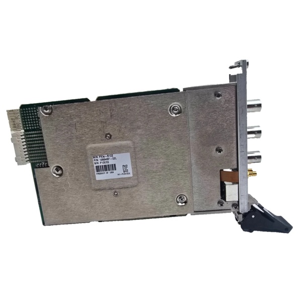
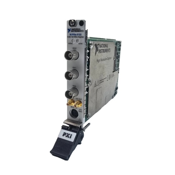
- Connectors: BNC (CH0, CH1, TRIG); SMB (CLK IN/OUT); 9-pin mini-circular DIN (AUX I/O)
- Trigger Types: Edge, hysteresis, window, video (NTSC/PAL/SECAM), digital, software
- Trigger Jitter: ≤80 ps rms
- Input Overload: 50 Ω: 7 Vrms (peaks ≤10 V); 1 MΩ: peaks ≤42 V
- Operating Temperature: 0°C to 55°C (0-45°C in PXI-1000/B and PXI-101x chassis)
- Storage Temperature: -40°C to 71°C
- Relative Humidity: 10% to 90% noncondensing
- Power Draw: +12 V @ 2.32 A max, +3.3 V @ 1.6 A max; total power 33.12 W max
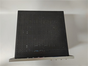
- Dimensions: 3U one-slot PXI Express module, 21.3 cm × 2.0 cm × 13.0 cm
- Weight: 453 g (16.0 oz)
- Isolation Rating: Not applicable (single-channel isolation not provided; ground-referenced inputs)
- Calibration Interval: 2 years
- Compliance: IEC 61010-1, EN 61326-1, FCC Part 15B Class A
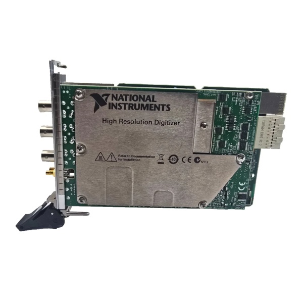
NI PXIe-5122 (779967-03)
The Real-World Problem It Solves
Traditional 8-bit benchtop oscilloscopes lack the vertical resolution and data streaming capability for high-dynamic-range, long-duration acquisitions in automated test systems. The PXIe-5122 delivers 14-bit resolution with 400 MB/s sustained streaming to PC memory or RAID storage, eliminating the need for separate digitizers and streaming hardware while maintaining low-noise performance for frequency-domain analysis.
Where you’ll typically find it:
- Signal intelligence and SIGINT streaming IF/RF data at 400 MB/s for spectrum analysis
- Radar and ultrasound applications requiring >1 million triggered waveforms with 100 ps timestamp resolution
- Automotive ECU testing synchronizing multiple modules for high-channel-count mixed-signal measurements
Bottom line: This oscilloscope replaces a benchtop scope + streaming digitizer + external trigger router in one PXI slot, delivering 14-bit resolution with PXI bus synchronization for multi-instrument test systems.
Hardware Architecture & Under-the-Hood Logic
The PXIe-5122 is built on NI’s Synchronization and Memory Core (SMC) architecture, featuring dual 14-bit ADCs sampled at 100 MS/s with deep onboard memory and PXI Express x4 interface for high-speed data transfer. The module includes software-selectable 50 Ω/1 MΩ input impedance, programmable gain stages, anti-alias and noise filters, and an FPGA for real-time signal processing, triggering, and data buffering to onboard memory. The PXIe x4 interface enables 400 MB/s sustained streaming to host memory or RAID storage. A low-jitter 100 MHz clock generator distributes timing signals with <10 ps skew between channels, supporting external reference clocks and NI-TClk for multi-module synchronization.
- Analog input signals (CH0, CH1, TRIG) enter through front-panel BNC connectors → Software-selectable 50 Ω/1 MΩ impedance with AC/DC/GND coupling (AC coupling only on 1 MΩ) → Programmable vertical offset circuitry → Variable gain amplifier adjusts to selected input range (0.2 V to 20 Vpk-pk)
- 14-bit ADC core samples analog inputs at up to 100 MS/s real-time or 2 GS/s RIS (repetitive signals) → Digitized data stored in deep onboard memory (8-256 MB per channel) → FPGA controls acquisition, triggering, and data management
- Trigger system: Analog trigger (edge, hysteresis, window) on CH0, CH1, TRIG → Video trigger (NTSC, PAL, SECAM) with line/field selection → Digital triggers via PXI_Trig backplane and PFI0/PFI1 → Trigger comparator with <80 ps jitter
- Data path: Acquired waveforms in onboard memory → PXI Express x4 interface transfers data at up to 400 MB/s to host controller → Streaming to PC memory, hard disk, or RAID 0 arrays for long acquisitions
- Clock distribution: Internal VCXO provides 100 MHz timebase (±25 ppm accuracy) → External reference clock via CLK IN (30-105 MHz) or PXI Star Trigger (30-80 MHz) → PLL locks internal clock to reference for synchronized multi-module systems
- Synchronization: PXI trigger bus routes trigger signals → PFI lines provide programmable function interface for external trigger/event I/O → Sample clock export via CLK OUT (up to 105 MHz) and PXI_Trig (up to 20 MHz)
- Memory management: Deep onboard memory (up to 256 MB/channel) → Multiple-record mode acquires >1 million triggered waveforms without software intervention → 100 ps timestamp resolution for each triggered event
- Filtering: Software-selectable noise filter (2-pole Bessel, 20 MHz), anti-alias filter (6-pole Chebyshev, 35 MHz), or filters off → AC coupling cutoff at 12 Hz (1 MΩ only)
- Calibration: Self-calibration corrects gain, offset, frequency response, triggering, and timing for all input ranges → Onboard voltage reference provides stability over 0-55°C operating range → External calibration interval 2 years
- Power and thermal: PXIe backplane provides power (<33 W max) → Thermal management through forced-air cooling via chassis fans → Operating temperature 0-55°C (0-45°C in PXI-1000/B and PXI-101x chassis) with thermal protection
NI PXIe-5122 (779967-03)
Field Service Pitfalls: What Rookies Get Wrong
Exceeding 50 Ω Input Overload Limits
Connecting signals exceeding 7 Vrms or 10 V peaks to 50 Ω input damages the front-end attenuation network. The 20 V range is only available on 1 MΩ input—50 Ω input maximum overload is 7 Vrms with peaks ≤10 V regardless of selected range.
- Field Rule: Verify impedance setting before applying signals. Use 1 MΩ input for signals up to 20 Vpk-pk. On 50 Ω, maximum signal is 7 Vrms with peaks ≤10 V. Check the vertical scale and impedance before power-up.
Bandwidth Degradation Above 40°C
Operating above 40°C ambient temperature reduces analog bandwidth to 78 MHz for all ranges except 0.2 V, causing amplitude errors for signals approaching 100 MHz. The datasheet explicitly states “78 MHz above 40°C”—this is a warranted specification.
- Quick Fix: Monitor chassis inlet temperature. If ambient exceeds 40°C, reduce test signal frequency below 78 MHz or account for bandwidth limitation in measurements. For critical high-frequency measurements, maintain chassis temperature below 40°C using adequate cooling.
Assuming RIS Provides Real-Time 2 GS/s Capture
Random interleaved sampling (RIS) achieves 2 GS/s effective sampling only for repetitive signals by acquiring multiple samples from multiple trigger events. Single-shot transient events cannot be captured at 2 GS/s; maximum real-time sampling is 100 MS/s.
- Field Rule: Use RIS only for repetitive signals stable across multiple trigger events. For single-shot transients, the maximum effective sampling rate is 100 MS/s. For unique event capture at higher rates, consider a higher-bandwidth digitizer.
SFDR Degradation on Higher Voltage Ranges
SFDR degrades to 65 dBc on 4 V range and 60 dBc on 10 V/20 V ranges (1 MΩ), increasing harmonic distortion visibility in spectral analysis. For applications requiring maximum dynamic range, using higher ranges compromises measurement integrity.
- Field Rule: Match input range to signal amplitude for maximum SFDR. For >75 dBc SFDR, use 0.2 V to 2 V ranges. For 4 V or higher ranges, account for reduced SFDR (60-65 dBc) in spectral measurements.
Ignoring Trigger Jitter in Timing-Critical Measurements
At 100 MS/s (10 ns sample period), 80 ps trigger jitter represents 0.8% of the sample period, introducing timing uncertainty that degrades high-precision timing measurements like pulse width or inter-channel phase.
- Field Rule: Account for trigger jitter in timing-critical applications. The warranted trigger jitter is <80 psrms within ±5°C of self-calibration temperature. Perform self-calibration before critical measurements. For multi-module synchronization, lock all modules to the same external reference clock to minimize inter-channel skew.
Commercial Availability & Pricing Note
Please note: The listed price is for reference only and is not binding. Final pricing and terms are subject to negotiation based on current market conditions and availability.