Description
Hard-Numbers: Technical Specifications
- Bandwidth: DC to 6 GHz
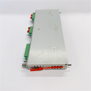
- Switch Configuration: 18×1 2-port bidirectional multiplexer
- Number of Channels: 18 input channels, 1 common output (2-port configuration)
- Impedance: 50 Ω
- Insertion Loss: < 0.5 dB at 3 GHz
- VSWR (Voltage Standing Wave Ratio): < 1.5:1 at 3 GHz
- Switching Time: < 250 μs (typical)
- Repeatability: < 0.05 dB
- Isolation: > 70 dB at 3 GHz
- Power Handling: +30 dBm (1 W) continuous
- Channel-to-Channel Crosstalk: > 60 dB at 3 GHz
- Operating Temperature: 0°C to 50°C
- Storage Temperature: -40°C to 70°C
- Power Requirements: +5 VDC, +3.3 VDC, -52 VDC (from PXIe backplane)
- Power Consumption: Typical 18 W, maximum 25 W
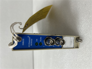
- Connector Type: SMA (female) on front panel
- Module Type: PXI Express (Hybrid PXI/PXIe compatible)
- Bus Interface: PXIe Gen 1 x1 lane (250 MB/s)
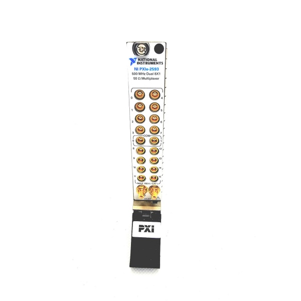
NI PXIe-2593
The Real-World Problem It Solves
Traditional RF switching matrices require external rack-mounted coaxial switches, adding cabling complexity and signal degradation in high-frequency test systems. The PXIe-2593 integrates an 18×1 RF multiplexer directly into the PXIe chassis, delivering 6 GHz bandwidth with bidirectional routing and minimizing signal path length. This eliminates external switch boxes, reduces insertion loss, and maintains signal integrity for RF/microwave test applications.
Where you’ll typically find it:
- Wireless device testing: Routing RF signals between DUTs (Device Under Test) and test equipment in production ATE systems
- Aerospace/defense RF testing: Switching radar and communication signals in multi-port antenna testing
- RF component characterization: Automating S-parameter measurements for filters, amplifiers, and antennas
Bottom line: This module consolidates RF switching into the PXIe platform, reducing test system footprint while maintaining 6 GHz signal integrity and bidirectional routing capability.
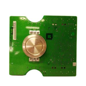
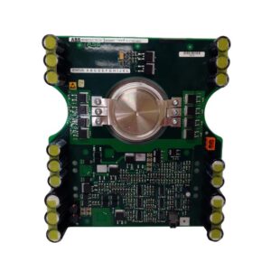
Hardware Architecture & Under-the-Hood Logic
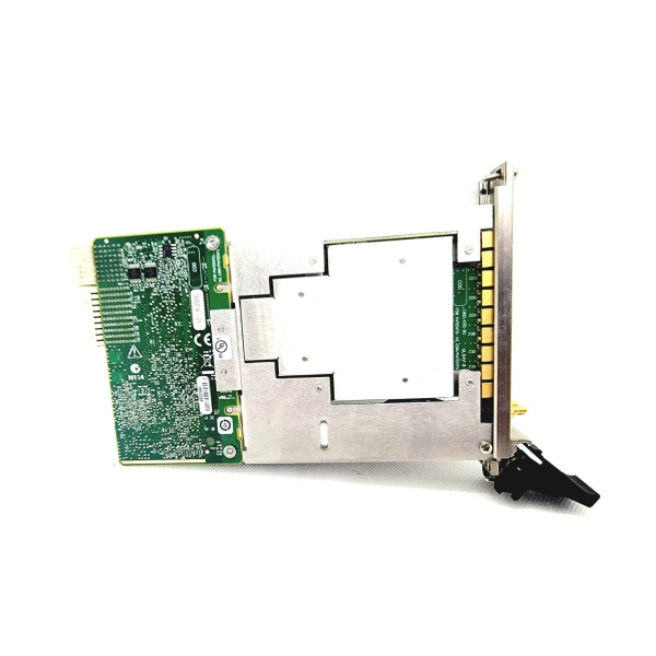
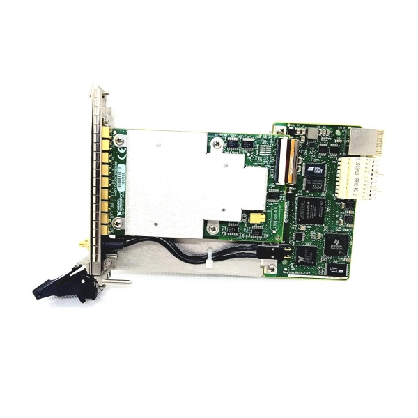
The PXIe-2593 is a 3U PXI Express module containing an RF switching matrix based on solid-state RF switch technology. The module features 18 input channels with SMA connectors on the front panel, routed through bidirectional RF switches to a 2-port common output. The switching matrix is controlled via FPGA-based logic that manages switch sequencing and ensures minimal switching time (< 250 μs). The RF path is designed with 50 Ω characteristic impedance throughout, with impedance-matched traces and connectors to minimize VSWR (< 1.5:1 at 3 GHz). The module draws power from the PXIe backplane (+5 V, +3.3 V, -52 V rails) and integrates filtering and regulation for clean RF switching.
- RF input signals (18 channels) enter through front-panel SMA connectors → routed through bidirectional solid-state RF switches
- FPGA controller receives switch commands via PXIe bus interface (Gen 1 x1, 250 MB/s) → generates control signals for RF switch matrix
- RF switch matrix routes selected input channel to 2-port common output → maintains 50 Ω impedance throughout signal path
- Signal path design uses impedance-matched traces and low-loss RF materials → minimizes insertion loss (< 0.5 dB at 3 GHz) and VSWR
- Power distribution from PXIe backplane (+5 V, +3.3 V, -52 V) → filtered and regulated for RF switch circuitry
- Thermal management through conduction cooling to chassis → maintains performance in 0°C to 50°C operating temperature range
- Switch timing controlled by FPGA → ensures < 250 μs switching time with < 0.05 dB repeatability
NI PXIe-2593
Field Service Pitfalls: What Rooks Get Wrong
Overestimating Power Handling Capacity
Rookies assume the PXIe-2593 can handle high-power RF signals indefinitely, ignoring the +30 dBm (1 W) continuous rating. Connecting high-power amplifiers or transmitters exceeding this limit can damage the RF switches, especially at high duty cycles or continuous wave (CW) operation.
Field Rule: Verify RF signal power at the module input does not exceed +30 dBm continuous. Use external attenuators if necessary—calculate required attenuation: Attenuator (dB) = Signal Power (dBm) – 30 dBm. Remember: peak power handling may be higher than continuous rating, but derate for duty cycle > 10%. Monitor module temperature in NI MAX; unexpected temperature rise indicates excessive RF power dissipation.
Neglecting Impedance Mismatch Losses
Engineers connect the PXIe-2593 to test equipment or DUTs with non-50 Ω impedance (75 Ω or 75/50 Ω mixed systems), causing VSWR degradation and signal reflection. The module is designed for 50 Ω systems only; impedance mismatch introduces measurement error and can damage switches at high power levels.
Quick Fix: Verify entire signal path is 50 Ω impedance—DUT, cables, connectors, and test equipment. Use 50 Ω to 75 Ω impedance transformers only if absolutely necessary (they introduce 6 dB loss). Measure VSWR with a vector network analyzer (VNA) at each connection; if VSWR > 1.5:1 at 3 GHz, identify and correct mismatch. For mixed impedance systems, consider external impedance-matching networks rather than relying on the PXIe-2593’s internal impedance.
Ignoring Insertion Loss in High-Frequency Measurements
Technicians assume insertion loss is negligible across the entire DC-6 GHz bandwidth, ignoring the frequency-dependent loss characteristic. Insertion loss increases with frequency—< 0.5 dB at 3 GHz, but can exceed 1.5 dB near 6 GHz—causing measurement error in gain, noise figure, and S-parameter measurements.
Field Rule: Characterize insertion loss of the PXIe-2593 at your test frequencies before critical measurements. Use a VNA to measure S21 (forward transmission) through the module with all switches in the same state. Subtract measured insertion loss from test results to correct for module loss. For high-accuracy measurements (> ±0.1 dB), create a calibration routine that accounts for frequency-dependent insertion loss—store the correction table in your test software and apply it during post-processing.
Commercial Availability & Pricing Note
Please note: The listed price is for reference only and is not binding. Final pricing and terms are subject to negotiation based on current market conditions and availability.