Description
Hard-Numbers: Technical Specifications
- Analog Inputs: 8 channels, 16-bit, 750 kS/s per channel (dedicated ADC per channel)
- Analog Outputs: 8 channels, 16-bit, 1 MS/s update rate, ±10 V range
- Digital I/O: 96 bidirectional lines configurable as inputs, outputs, counters, or custom logic
- Digital I/O Speed: Up to 40 MHz operation
- FPGA Type: Xilinx Virtex-5 LX50
- FPGA Resources: 28,800 flip-flops, 48 DSP slices, 1,728 kbits block RAM
- Timebase: 40, 80, 120, 160, or 200 MHz programmable
- DMA Channels: 3 channels for high-speed data streaming
- Analog Input Range: ±10 V (software selectable)
- ADC Conversion Time: 1 μs
- DAC Update Time: 1 μs
- Input Impedance: 10 GΩ (powered), 4.0 kΩ (unpowered)
- Overvoltage Protection: ±42 V (powered), ±35 V (unpowered)
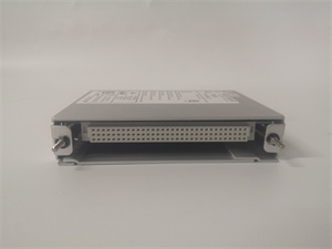
- I/O Connectors: 3 × 68-pin female VHDCI
- Operating Temperature: 0°C to 55°C (32°F to 131°F)
- Power Requirements: +3.3 V @ 847 mA, +12 V @ 0.5 A

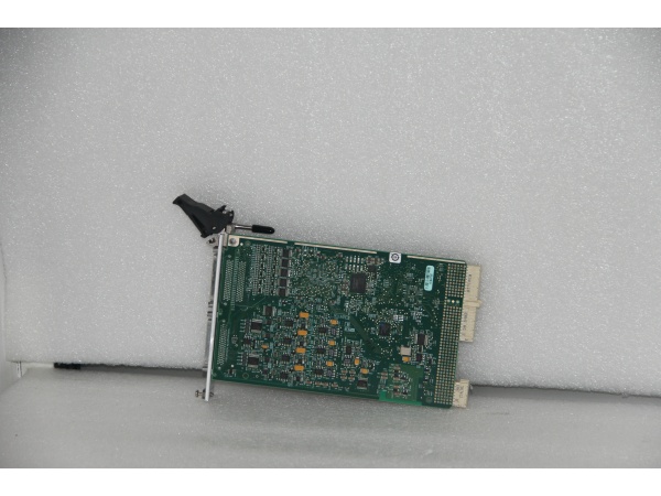
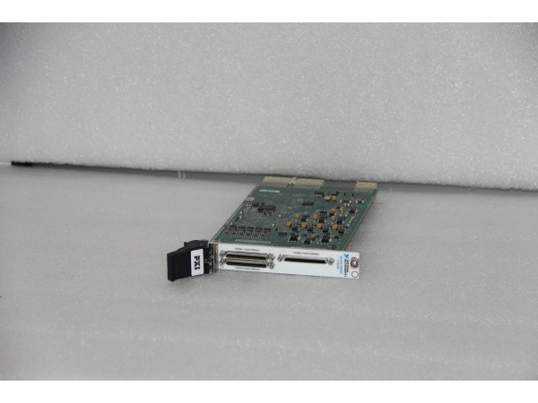
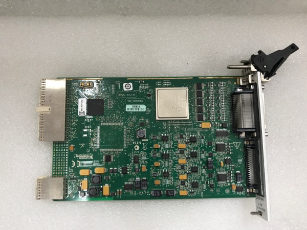
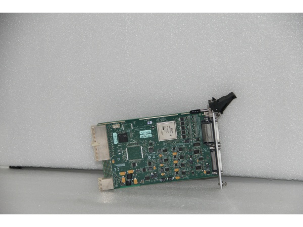
NI PXI-7852R
The Real-World Problem It Solves
When standard DAQ cards can’t meet your timing requirements or you need custom protocols that don’t exist off the shelf, the FPGA lets you roll your own hardware logic in LabVIEW. Dedicated ADCs per channel mean each input samples independently—no multiplexing, no skew, no excuses.
Where you’ll typically find it:
- Hardware-in-the-loop (HIL) test rigs for ECU and powertrain validation
- Sensor simulation for avionics and automotive black-box testing
- Custom digital protocol emulation (I2C, SPI, MIL-STD-1553, proprietary protocols)
- High-speed control loops with sub-microcycle response requirements
Bottom line: It’s a blank canvas of high-speed I/O backed by a serious FPGA—if you can dream it in LabVIEW FPGA, this hardware will execute it with deterministic timing.
Hardware Architecture & Under-the-Hood Logic
The PXI-7852R centers on a Xilinx Virtex-5 LX50 FPGA that connects directly to dedicated analog and digital I/O blocks. Each analog input has its own 16-bit SAR ADC, eliminating multiplexer delays and enabling per-channel independent sampling and triggering.
Signal flow and processing logic:
- PXI Bus Interface: Host PC communicates via PXI bus using NI-RIO driver.
- FPGA Execution Engine: LabVIEW FPGA code compiles to bitstream running on Virtex-5 LX50.
- Analog Input Path: Each of 8 channels routes to dedicated ADC (1 μs conversion time).
- Analog Output Path: 8 DACs update at 1 MS/s with ±10 V output range.
- Digital I/O Matrix: 96 lines connect to FPGA fabric with 40 MHz toggle capability.
- DMA Engines: 3 DMA channels stream data between FPGA memory and host RAM.
- PXI Trigger Bus: PXI/TRIG lines 0-7 for chassis-wide synchronization.
- PXI/STAR Access: Star trigger bus access (avoid slot 2 per manual warning).
- PXI/CLK10: 10 MHz chassis clock for multi-device phase locking.
NI PXI-7852R
Field Service Pitfalls: What Rookies Get Wrong
Burning FPGA with Wrong Compile Target
LabVIEW FPGA projects often target the wrong FPGA variant or compile for PCIe when using PXI. The bitstream loads but timing fails or resources run out, causing flaky behavior that’s hard to debug.
- Field Rule: Always verify the compile target matches your exact hardware (PXI-7852R, not PCIe-7852R). Check resource utilization after compile—Virtex-5 LX50 has limits. If you’re over 90% slice or BRAM usage, optimize before deploying to production.
Ignoring Ground Reference Differences
The three 68-pin connectors share digital ground but analog I/O needs separate returns. Mixing grounds causes noise that shows up as jitter in high-speed digital or low analog readings.
- Quick Fix: Use Analog Input Ground and Analog Output Ground pins exclusively for analog signals. Never reference analog circuits to digital ground—keep them separate all the way to your field wiring.
Overloading the +12 V Rail
The module draws 0.5 A from +12 V on the PXI backplane. Adding external loads to this rail or stacking too many high-power cards starves the FPGA and causes brownouts or random reboots.
- Field Rule: Never tap +12 V for external devices. If you need field power, use an external supply. Monitor PXI backplane current during commissioning—if you see voltage dips under load, redistribute power across chassis slots.
Writing to PXI/STAR from Slot 2
The manual explicitly warns against using PXI/STAR when the card is in chassis slot 2. It corrupts the 10 MHz clock timing and crashes the PXI system.
- Field Rule: Check chassis slot assignment before deploying code. If PXI-7852R lands in slot 2, either move it to another slot or disable PXI/STAR access in your FPGA code. Don’t assume—verify slot position physically and in MAX.
Assuming Digital Lines Are 5 V Tolerant
The digital I/O operates at 3.3 V logic levels by default. Applying 5 V signals without configuration can damage the FPGA I/O buffers over time.
- Field Rule: Configure digital I/O voltage levels in LabVIEW FPGA project before deployment. If interfacing to 5 V logic, use level shifters or verify the FPGA I/O bank supports 5 V tolerance—don’t guess and fry the chip.