Description
Hard-Numbers: Technical Specifications
- Output Channels:
- Channel 0: 0 V to +6 V (non-isolated), 1 A maximum (6 W)
- Channel 1: 0 V to +20 V (isolated from chassis ground), 20 mA / 1 A ranges (2 W / 20 W)
- Channel 2: 0 V to -20 V (isolated from chassis ground), 20 mA / 1 A ranges (2 W / 20 W)
- Voltage Programming Accuracy/Resolution (1 year, 23°C ± 10°C):
- Channel 0 (±6 V): 0.12 mV resolution, 0.05% + 4 mV accuracy, tempco 0.005% + 0.3 mV/°C
- Channels 1/2 (±20 V): 0.40 mV resolution, 0.05% + 10 mV accuracy, tempco 0.005% + 1 mV/°C
- Current Programming Accuracy/Resolution (1 year, 23°C ± 10°C):
- Channel 0 (1 A range): 0.02 mA resolution, 0.15% + 4 mA accuracy, tempco 0.02% + 0.2 mA/°C
- Channels 1/2 (20 mA range): 0.40 μA resolution, 0.15% + 60 μA accuracy, tempco 0.01% + 3 μA/°C
- Channels 1/2 (1 A range, with auxiliary power): 0.02 mA resolution, 0.15% + 4 mA accuracy, tempco 0.02% + 0.2 mA/°C
- Voltage Measurement Accuracy/Resolution:
- Channel 0 (±6 V): 0.06 mV resolution, 0.05% + 4 mV accuracy
- Channels 1/2 (±20 V): 0.20 mV resolution, 0.05% + 5 mV accuracy
- Current Measurement Accuracy/Resolution:
- Channel 0 (1 A range): 0.01 mA resolution, 0.15% + 4 mA accuracy
- Channels 1/2 (20 mA range): 0.20 μA resolution, 0.15% + 35 μA accuracy
- Channels 1/2 (1 A range, with auxiliary power): 0.01 mA resolution, 0.15% + 4 mA accuracy
- Output Speed (Typical):
- Channel 0: Rise/fall time <1 ms (full load, auxiliary power), <1 ms (full load, no load), <25 ms (no load, internal power)
- Channels 1/2: Rise/fall time <1 ms (full load, auxiliary power), <2 ms (full load, no load), <20 ms / <10 ms (no load, auxiliary power)
- Channels 1/2 (internal power, 1 A range not available): 20 mA range only, up to 100 mA maximum combined
- Ripple and Noise (Typical):
- RMS normal-mode voltage (20 Hz to 20 MHz): <1.5 mV (Channel 0), <1 mV (Channels 1/2)
- RMS normal-mode current: <8 μA (Channel 0), <8 μA (Channels 1/2, 1 A range), <3 μA (Channels 1/2, 20 mA range)
- Transient Response: Recovers to <0.1% of voltage range within 50 μs after a load current change from 50% to 100% of range (typical)
- Measurement Timing:
- Default sample rate: 300 S/s nominal
- Maximum sample rate: 3,000 S/s nominal
- Power Requirements:
- PXI power: 10 W at 5 V, 1 W at 3.3 V, 6 W at 12 V, 3 W at -12 V (typical)
- Auxiliary power (optional, channels 1 and 2 only): 11 VDC to 15.5 VDC, 5 A maximum, ≥60 W recommended
- Protection:
- Overvoltage tolerance: 14 VDC over rated output per channel (CAT I)
- Overcurrent / reverse voltage: Fused
- Overtemperature: Automatic shutdown
- Auxiliary power overvoltage: >15.5 VDC shut-off, >20 VDC crowbar (fused)
- Isolation: Channels 1 and 2 isolated from earth ground at 60 VDC, CAT I (verified by dielectric withstand test, 5 s continuous). Channel 0 is non-isolated (common with chassis ground). Channels 1 and 2 not isolated from each other.
- Absolute Maximum Limits:
- Maximum voltage (channel-to-COM): 14 VDC over rated output, CAT I
- Cascading multiple channels, channel-to-chassis ground: 60 VDC maximum
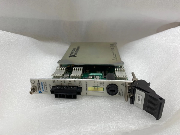
- Physical Characteristics:
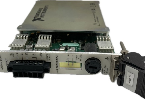
- Dimensions: 3U, one-slot PXI/cPCI module, 2.0 × 13.0 × 21.6 cm (0.8 × 5.1 × 8.5 in.)
- Weight: 323 g (11.4 oz)
- I/O connectors: MINI-COMBICON, 3.81 mm (6-position) for outputs; MINI-COMBICON, 3.5 mm (2-position) for auxiliary power input
- User-replaceable fuses:
- Output channels (internally socketed): 3 × Littelfuse 045301.5 (F 1.5 A 125 V), characteristic
- Auxiliary power input (front panel mount): 1 × Littelfuse 21806.3 (T 6.3 A L250 V), characteristic
- Environment:
- Operating temperature: 0°C to +55°C
- Storage temperature: -40°C to +71°C
- Relative humidity (operating): 10% to 90%, noncondensing
- Relative humidity (storage): 5% to 95%, noncondensing
- Maximum altitude: 2,000 m (at 25°C ambient)
- Pollution Degree: 2, indoor use only
- Shock and Vibration:
- Operational shock: 30 g peak, half-sine, 11 ms pulse (IEC 60068-2-27, MIL-PRF-28800F test profile)
- Random vibration (operating): 5 Hz to 500 Hz, 0.31 grms (IEC 60068-2-64)
- Random vibration (nonoperating): 5 Hz to 500 Hz, 2.46 grms (IEC 60068-2-64)
- Compliance:
- Safety: IEC 61010-1, EN 61010-1, UL 61010-1, CSA C22.2 No. 61010-1
- EMC: EN 61326-1 (Class A emissions, basic immunity), EN 55011/22/24 (CISPR 11/22/24), FCC 47 CFR Part 15B (Class A), ICES-001 (Class A)
- CE: 2014/35/EU (LVD), 2014/30/EU (EMC), 2011/65/EU (RoHS), 2014/53/EU (RED), 2014/34/EU (ATEX)
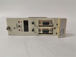
NI PXI-4110 779647-11
The Real-World Problem It Solves
Many automated test systems need multiple precision DC voltage rails—positive, negative, and low-voltage logic bias—to power DUTs or simulate battery sequences. Traditional bench power supplies take up rack space, lack programmability, and can’t be synchronized with PXI measurement instruments. The PXI-4110 packs three independent outputs into a single 3U slot, offering fast voltage/current programming, high-resolution readback, and hardware-triggered synchronization with other PXI modules. It’s the difference between manually tweaking three bench supplies and a fully automated, synchronized power-sequencing system that ramps voltages, measures currents, and logs data without human intervention.
Where you’ll typically find it:
- Semiconductor Characterization: Biasing op-amps or ADCs with ±20 V rails while providing +6 V reference voltages, with precise current measurement for quiescent current analysis
- Automotive ECU Testing: Simulating battery voltage profiles (sag, surge, cranking) on +12/+24 V rails while providing logic-level biasing for CAN transceivers
- Consumer Electronics Power-On/Off Sequencing: Applying +20 V, -20 V, and +6 V rails in precise sequences to verify power supply integrity, inrush current limits, and brownout recovery behavior
Bottom line: This module is your programmable triple-rail DC source in a PXI slot. When it fails, your multi-rail testing capability dies—you can’t bias analog front-ends, simulate battery profiles, or sequence power rails automatically. Keep a spare on the shelf, especially if your test fixtures depend on its isolation properties.
Hardware Architecture & Under-the-Hood Logic
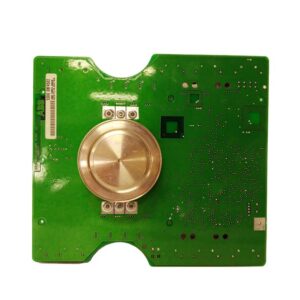
The PXI-4110 is a 3U PXI module containing three independent DC power supply channels based on a hybrid linear/switching architecture. Channel 0 (0 to +6 V, non-isolated) uses a Linear Technology LT1773 boost-buck switching preregulator combined with an LT1970 power op-amp linear output stage, providing both efficiency and low noise. Channels 1 (0 to +20 V) and 2 (0 to -20 V) are isolated from chassis ground and use high-power DC-DC converters (approximately 200 kHz switching frequency) as preregulators feeding LT1970-based linear output stages. The LT1970 power op-amp with precision current limit forms the heart of each channel’s voltage/current control block, giving SMU-like behavior (constant voltage or constant current operation depending on load). An FPGA synthesizes the drive signals for switching MOSFETs, manages PID control loops for the preregulators, and coordinates measurement ADCs (200 kS/s, 16-bit). Auxiliary power (optional, 11–15.5 VDC, ≥60 W) can be connected to boost channels 1 and 2 from 20 mA to 1 A output current capability; without it, these channels are limited to 20 mA maximum each (combined ≤3 W total from PXI backplane). All channels support 16-bit voltage setpoint and current limit programming, with integrated voltage/current measurement readback. Protection includes programmable voltage/current limits, output fuses, overtemperature shutdown, and tolerance for reverse-polarity voltage application.
- Host software sends command via PXI bus (e.g., niDCPower_ConfigureVoltageLevel or niDCPower_ConfigureCurrentLimit) specifying channel, voltage level, and current limit
- FPGA decodes command and routes to appropriate channel control block—for channels 1/2, also determines whether to use internal PXI backplane power (limited to 20 mA range) or auxiliary power (enables 1 A range)
- PID control loop in FPGA adjusts switching preregulator duty cycle—LT1773 for channel 0, high-power DC-DC converters for channels 1/2—to maintain optimal headroom above programmed output voltage
- LT1970 power op-amp receives setpoint from FPGA and drives discrete MOSFET output devices to regulate linear output voltage to target with millisecond-level settling time
- Current sense circuitry monitors output current via shunt resistors, feeding back to LT1970 for precision current limiting (constant-current mode when load draws more than programmed limit)
- Measurement ADCs (200 kS/s, 16-bit) continuously sample output voltage and current from each channel—default averaging of 300 samples for optimal 50/60 Hz noise rejection, user-configurable up to 3,000 S/s
- Data transmitted via PXI backplane (132 MB/s bandwidth) to host controller—latency in microsecond range vs. milliseconds for traditional GPIB/RS-232 instruments
- Protection circuitry monitors continuously—overvoltage (tolerates 14 VDC over rated output), overcurrent (fused at 1.5 A per channel), reverse-polarity voltage (fused), overtemperature (automatic shutdown requiring software reset)
- Trigger I/O synchronization enables coordinated voltage ramps or current steps with other PXI instruments (e.g., DMM measurement triggers aligned with power supply output changes via PXI trigger lines 0–7)
- Auxiliary power management—when connected (11–15.5 VDC, ≥60 W), channels 1/2 can deliver 1 A; if lost during operation, isolated outputs disable and supply shuts down to prevent damage
NI PXI-4110 779647-11
Field Service Pitfalls: What Rookies Get Wrong
Assuming Channels 1 and 2 Can Deliver 1 A Without Auxiliary Power
Rookies see the “1 A” spec in the datasheet and assume all three channels deliver 1 A from PXI backplane power. Channels 1 and 2 are limited to 20 mA maximum each when using internal PXI power, with combined output ≤3 W total. The 1 A capability on these channels requires connecting an auxiliary 11–15.5 VDC, ≥60 W power source to the front-panel connector. Attempting to draw >20 mA from channels 1/2 without auxiliary power causes voltage sag, current limiting, or module shutdown due to PXI backplane power budget exceeded.
Field Rule: Check your application’s current requirements. If you need >20 mA on channels 1 or 2, connect an external 12 VDC power supply (NI APS-4100 recommended) to the auxiliary power input. Verify auxiliary power is present by reading the Power Source In Use attribute or checking front-panel LED (if equipped). If auxiliary power fails during operation, channels 1 and 2 automatically disable—reset the supply via niDCPower_Reset after restoring power.
Overlooking Isolation Limitations Between Channels 1 and 2
Techs assume channels 1 and 2 are isolated from each other because both are isolated from chassis ground. They’re not—isolation is only channels 1/2 to earth ground (60 VDC, CAT I). If you connect channel 1 to +20 V referenced to chassis ground, then connect channel 2 to a load also referenced to chassis ground, you create a ground loop or potentially exceed isolation ratings if external circuitry has ground offsets. This can cause measurement errors, noisy outputs, or damage if isolation barriers are exceeded.
Quick Fix: Treat channels 1 and 2 as isolated from chassis ground but not from each other. If you need true channel-to-channel isolation, use separate PXI-4110 modules or other isolated power supplies. For most applications, the isolation to earth ground is sufficient—just don’t assume channels 1 and 2 can float independently relative to each other. Document ground reference schemes in your test plan and verify with a multimeter that channels 1 and 2 share a common (non-earth) reference.
Ignoring Calibration Warm-Up Time for Precision Measurements
Rookies power on the PXI-4110 and immediately start high-accuracy voltage/current measurements. The specs are guaranteed only after a 15-minute warm-up time. Cold-start measurements drift as internal components stabilize, especially critical for low-current (<1 mA) or low-voltage (<1 V) measurements where accuracy offsets dominate. You’ll see measurement drift over the first 10–15 minutes that falsely suggests DUT parameter shift or instability.
Field Rule: Allow 15 minutes of warm-up before precision measurements. For automated test sequences, program a delay at power-up or use the module’s self-test as a warm-up indicator before proceeding to critical measurements. Calibration interval is 1 year—track calibration dates and don’t rely on uncalibrated modules for accuracy-critical applications. If you need faster turn-on, verify warm-up characteristics for your specific accuracy requirements via characterization.
Forgetting That Channel 0 Is Non-Isolated
Channel 0 (0 to +6 V) shares a common reference with chassis ground—it’s not isolated. Rookies treat it like an isolated channel and connect it to circuitry floating at high potentials relative to chassis ground, or they cascade it with channels 1/2 without respecting the 60 VDC maximum channel-to-chassis ground limit. This creates ground loops, measurement errors, or potential safety hazards if floating potentials exceed isolation ratings.
Quick Fix: Treat channel 0 as chassis-ground-referenced. If you need a floating +6 V supply, use a different isolated module or ensure your DUT circuitry is also chassis-ground-referenced. When cascading channels for higher voltage (e.g., stacking +20 V and -20 V for 40 V), respect the 60 VDC maximum channel-to-chassis ground limit—never exceed this or isolation barriers can break down. Document channel grounding schemes and verify with a multimeter before connecting sensitive loads.
Misunderstanding Transient Response in High-Speed Applications
Techs assume the <1 ms rise/fall time spec applies universally. Full-load transient response is <1 ms with auxiliary power, but no-load response on internal power can be much slower (up to 25 ms for channel 0, up to 56 ms for channels 1/2). In high-speed sequencing applications (e.g., battery voltage sag simulation where you need millisecond-level steps), using internal power without auxiliary power causes sluggish response and missed timing windows—your test sequences won’t match the intended waveform.
Field Rule: Match your transient response requirements to power source. If you need fast rise/fall times (<2 ms) on channels 1/2, use auxiliary power. For channel 0, response is fast regardless of power source, but internal power slows no-load response significantly. Characterize your specific load conditions and verify transient response with an oscilloscope before committing to production test sequences. Use trigger synchronization (PXI trigger lines) to align measurement acquisition with power supply steps if timing is critical.
Overlooking Current Accuracy Derating Above 500 mA
Rookies assume the ±0.15% + 4 mA current accuracy applies at all current levels up to 1 A. Accuracy is derated for output currents >500 mA—the additional error percentage increases as you approach 1 A. At high currents (800 mA to 1 A), your actual accuracy is worse than the datasheet’s headline spec, leading to measurement errors in high-load applications (e.g., power supply validation at max current). You’ll think your measurement is within spec but it’s actually outside the derated accuracy curve.
Field Rule: Refer to the “Accuracy Specification Derating versus Output Current” graph in the datasheet. For currents >500 mA, apply the additional error percentage shown. If your application requires high accuracy at high current (±1% or better), consider calibrating the module at your specific operating points or using a higher-precision external shunt with DMM measurement. Document derating factors in your test uncertainty budget and don’t assume datasheet accuracy without checking current levels.
Commercial Availability & Pricing Note
Please note: The listed price is for reference only and is not binding. Final pricing and terms are subject to negotiation based on current market conditions and availability.