Description
Key Technical Specifications
- FPGA Core: It adopts Virtex – II V1000 FPGA. It has 10,240 flip – flops, 40 18×18 multipliers and 720Kbits embedded block RAM. The time base can be selected from 40MHz, 80MHz, 120MHz, 160MHz or 200MHz, enabling users to customize logic functions such as timing and triggering.
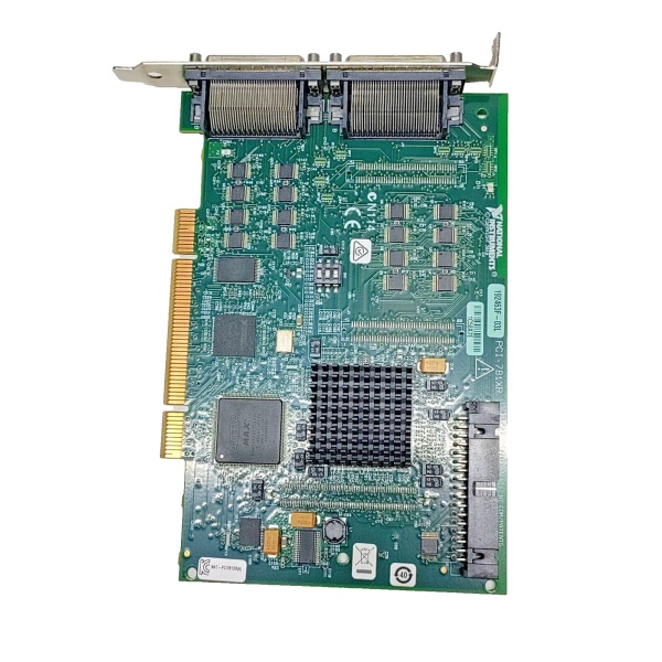
- Digital I/O Performance: It is equipped with 160 digital I/O lines. These lines can be flexibly configured as inputs, outputs, counters or custom logic interfaces. The output low voltage (VOL) is up to 0.4V when the output current is – 4mA, and the output high voltage (VOH) is at least 2.4V when the output current is 4mA, which is compatible with TTL – level signals.
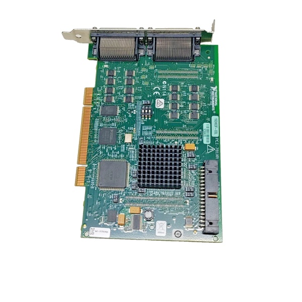
- Connectors & Interfaces: There are 4 68 – pin female high – density VHDCI connectors for signal wiring. It supports the RTSI bus, which has 8 shared trigger lines. Each line can be configured as input or output to realize synchronization with other devices that support the RTSI bus.
- Power & Physical Parameters: It works with +3.3VDC and +5VDC power supplies, with current requirements of 650mA and 9mA respectively. The physical size is 6.7 inches × 4.3 inches and the weight is only 0.25lb, which is compact and easy to install in the chassis.
- Software Compatibility: It requires NI – RIO 1.1 or later drivers. It supports LabVIEW 7.0 and above, and relies on the LabVIEW FPGA Module to customize and download virtual instruments to the FPGA. It is not compatible with Vivado software.

Part 4: Field Application & Problem Solved
In industrial automation and custom control scenarios, many traditional fixed – function I/O cards have problems such as inflexible function configuration and difficulty in synchronization with multiple devices. For example, in motor PWM control systems, different motors may require different timing and duty cycle parameters, and traditional I/O cards can only realize fixed – mode output and are difficult to adjust. In addition, when multiple test devices are used together, the lack of effective synchronization methods often leads to data deviation and control delay.
The NI PCI – 781XR solves these pain points through its reconfigurable characteristics and powerful synchronization capabilities. For instance, in an automobile assembly line’s motor control system, engineers can use the LabVIEW FPGA Module to program the FPGA on the PCI – 7811R to generate PWM signals with adjustable parameters. This allows the same card to control multiple types of motors, replacing multiple single – function control cards and reducing system complexity. In a petroleum industry’s DCS distributed control system, the card uses the RTSI bus to synchronize with temperature, pressure and other data acquisition modules. It ensures that the control signals and sensor data are time – aligned, which improves the accuracy of the production process control. Moreover, in small – batch customized production scenarios, its FPGA reconfigurability enables rapid function modification without replacing hardware, which shortens the production line transformation cycle.
Part 5: Installation & Maintenance Pitfalls (Expert Tips)
- FPGA Program Loading Misconfiguration: The SW1 switch on the device controls the loading of the FPGA program at startup. If SW1 is in the ON position, the VI stored in the flash memory will not be loaded when powered on. Novices may mistakenly toggle this switch, resulting in the failure of the device to work as expected. It is recommended to keep SW1 in the OFF position during normal operation.
- Incorrect Driver & Software Matching: The device relies on the NI – RIO driver, and the PCI – 7811R requires NI – RIO 1.1 or later. Installing an outdated driver or using software that does not match (such as Vivado) will cause the device to be unrecognized or fail to run. It is necessary to download the corresponding driver from NI’s official website and use LabVIEW and its FPGA Module for development.
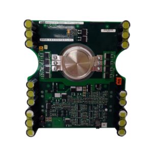
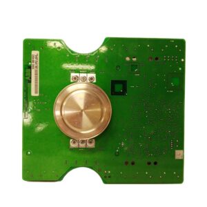
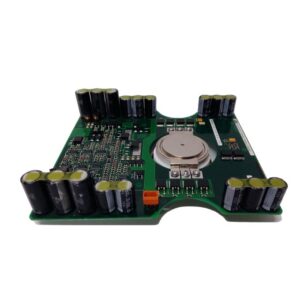
- Improper Wiring of Multi – connector: The device is equipped with 4 68 – pin VHDCI connectors. Wrong wiring between different connectors may lead to signal short circuits or I/O function failure. Before wiring, refer to the user manual to confirm the signal definition of each connector and use standard matching cables for connection.
- Neglecting RTSI Bus Conflict: When using the RTSI bus for multi – device synchronization, do not configure multiple devices to drive the same trigger line at the same time. This will cause signal conflicts and may damage the device. It is necessary to configure the input and output directions of each RTSI trigger line through software in advance to ensure that the signal flow is unique.
NI PCI-781XR
Part 6: Technical Deep Dive & Overview
The core advantage of the NI PCI – 781XR lies in the FPGA – driven reconfigurability, which allows users to customize the device’s functions according to specific needs instead of being restricted by fixed hardware logic. The Virtex – II V1000 FPGA it carries provides sufficient logic resources including multipliers and embedded RAM. These resources can support complex operations such as custom timing sequences, trigger logic and digital signal processing, and can even realize functions such as pulse code modulation encoding for remote telemetry applications.
The 160 digital I/O lines are the core I/O resources of the device. These lines can be flexibly configured as input, output or counter modes. Cooperating with DMA data streaming, they can realize high – speed transmission of large amounts of digital data and avoid data loss during the acquisition and control process. The RTSI bus is another key design. It realizes precise synchronization between the PCI – 781XR and other measurement devices through 8 shared trigger lines. This is crucial for scenarios that require collaborative work of multiple devices such as multi – channel data acquisition and multi – module linkage control.
In terms of usability, the device adopts a standard PCI slot design, which can be easily integrated into most industrial computers. The matching LabVIEW FPGA Module uses a graphical programming method, which lowers the threshold for users to program the FPGA. Even non – professional programmers can develop custom functions. However, the device also has limitations. Its FPGA model is relatively outdated, and it cannot support new high – performance programming tools. Moreover, it only provides digital I/O functions and lacks analog I/O capabilities. It needs to be used with analog acquisition cards in scenarios involving analog signals.
Overall, although the NI PCI – 781XR has been announced as a mature product, it still has irreplaceable value in maintaining legacy industrial control systems and small – batch custom control scenarios. Its balance of flexibility, compatibility and reliability has made it a classic choice in the field of reconfigurable I/O.