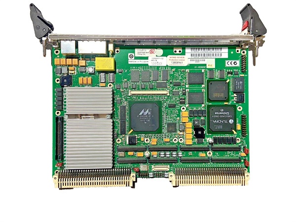
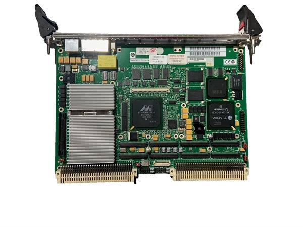
Description
Key Technical Specifications
-
Model Number: MVME6100-0161
-
Manufacturer: Motorola (now NXP/Emerson/Artesyn through acquisitions)
-
Product Family: MVME6100 Series VMEbus Processors (VME Renaissance flagship)
-
Form Factor: 6U VME (233.4 mm × 160 mm / 9.2″ × 6.3″)
-
Processor: Motorola/Freescale MPC7457 PowerPC RISC microprocessor at 1.267 GHz
-
Coprocessor: 128-bit AltiVec™ vector processing unit for parallel processing
-
Cache: 256 KB on-chip L2 cache, 2 MB L3 cache
-
Memory: 512 MB onboard DDR ECC SDRAM (expandable to 1-2GB via memory mezzanine)
-
Memory Bus: 133 MHz DDR memory bus with advanced host bridge matching
-
Storage: 128 MB Flash memory (dual 64 MB banks)
-
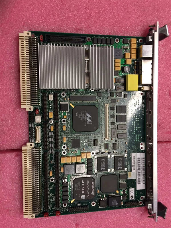
VMEbus Interface: Tundra Tsi148 VME interface chip with 2eSST (Dual Edge Source Synchronous Transfer) protocol
-
VME Bandwidth: 320 MB/s actual bandwidth (2eSST protocol)
-
PCI Buses: Two 64-bit PCI-X bus interfaces (133 MHz host bus)
-
PCI-X Configuration: One dedicated 100 MHz PMC support, one dedicated 133 MHz VME bridge
-
PMC Expansion: Dual 64-bit PMC-X slots (33/66/100 MHz capable)
-
PMCspan: PCI expansion connector for additional PMC interfaces via PCI6520 bridge
-
Ethernet: Dual Gigabit Ethernet (1000Base-T) interfaces
-
Serial Ports: Two RS-232/422/485 serial interfaces
-
System Controller: Marvell MV64360 (Discovery II) system controller with integrated peripherals
-
Power Supply: 5V DC ±5%, ±12V DC ±10%
-
Operating Temperature: -40°C to +85°C (industrial/military)
-
Storage Temperature: -40°C to +85°C
-
Humidity: 5% to 95% non-condensing
-
Vibration: 0.03 inch peak-to-peak, 10-500 Hz
-
Shock: 15G, 11 ms half-sine wave
-
Firmware: MOTLoad with POST, initialization, debugging, OS boot
-
Operating System Support: VxWorks, Linux, QNX
-
Migration Path: From MVME2300, MVME2400, MVME2600, MVME2700, MVME5100, MVME5500 series

Motorola MVME5500-0161
Field Application & Problem Solved
, delivering 320 MB/s actual bandwidth—4x the throughput of previous generations—while maintaining backward compatibility with existing VME backplanes and I/O cards.
where the combination of 1.267 GHz processing, AltiVec vector acceleration, and 320 MB/s VME throughput enables real-time processing of massive data streams.
uses both edges of the clock for data transfer, effectively doubling the data rate without requiring new backplane hardware—though it does require the Tsi148 interface chip and compatible VME64x backplanes. The dual Gigabit Ethernet
provides network-centric connectivity that matches the VME bus speed, eliminating the network bottleneck common in older designs. The DDR ECC memory
at 133 MHz provides the bandwidth to feed the processor and AltiVec unit without stalls. The dual PCI-X buses
—one for high-speed PMC modules, one dedicated to the VME bridge—prevent I/O contention and enable true parallel processing.
Installation & Maintenance Pitfalls (Expert Tips)
requires a VME64x-compliant backplane with proper signal integrity and termination. A common field mistake is installing the MVME6100-0161 in a legacy VME64 backplane and expecting 2eSST speeds. The board will fall back to standard VME64 modes (80 MB/s or less), negating the performance advantage. Check your backplane specifications for “VME64x” and “2eSST support” before installation. If your backplane is only VME64, consider upgrading or accept the bandwidth limitation. The Tsi148 chip
auto-negotiates, but you won’t see the 4x speedup without proper infrastructure.
provide redundant or aggregated network connectivity, but they require Gigabit-capable switches and proper cabling (Cat5e or Cat6). A common pitfall is connecting to 100 Mbps switches or using Cat5 cable, then wondering why network throughput doesn’t improve. Also, the dual ports can be configured for redundancy (failover) or aggregation (bonding)—verify your software configuration matches your network architecture. If using VxWorks, ensure you have the correct END driver for the Marvell MV64360 Ethernet controller
.
provides massive performance gains, but only if your code is compiled with AltiVec support and proper data alignment. AltiVec loads/stores require 16-byte aligned data—unaligned access causes exceptions or performance degradation. Use compiler flags (-maltivec for GCC, -qaltivec for XL C) and verify your data structures are padded to 16-byte boundaries. A common field issue is porting code from MVME5500 (which also had AltiVec) but forgetting that the MVME6100 has different cache line sizes and memory timing—reprofile and reoptimize for the new architecture.
. A frequent pitfall is installing 33 MHz PMC cards in the 100 MHz slot, or forcing 100 MHz with 66 MHz-only cards. The MVME6100 has two distinct PCI-X segments: one dedicated to PMC at 100 MHz, one dedicated to the VME bridge at 133 MHz
. Verify your PMC card specifications and set jumpers accordingly. The PMCspan expansion
adds more PMC slots via a PCI6520 bridge—ensure this bridge is properly configured or you’ll see enumeration errors.
. A dangerous pitfall is updating the primary boot image without verifying the backup image works. If the primary corrupts and the backup is blank or incompatible, the board bricks. Always maintain a known-good backup in the alternate bank. Use the S4 configuration switch
to select boot bank, and the write-protect jumpers to prevent accidental overwrites. The “Safe Start” header
forces default environment variables—use this if custom settings prevent boot.
, but this increases power dissipation and blocks airflow. A common mistake is installing the mezzanine in a chassis with marginal cooling, causing thermal throttling or shutdown. The mezzanine sits directly above the processor—ensure no cables obstruct the heatsink. If running at +85°C ambient
, verify your chassis has 200+ LFM airflow. Consider removing the mezzanine if not absolutely required for your application.
set these parameters. Multiple SCON boards cause bus arbitration conflicts; duplicate geographical addresses cause CR/CSR space collisions. Check your chassis documentation—some backplanes have fixed SCON slots. The MVME6100 uses the Discovery II VME bridge
—its CR/CSR mapping differs from older Universe II chips. Verify your VME window mappings if migrating from MVME5500 or earlier.
, the internal architecture differs significantly. The Tsi148 VME interface
has different programming models than the Universe II. VME DMA, interrupt handling, and CR/CSR access require driver updates. A common field issue is assuming MVME5500 VxWorks BSPs will work without modification—they won’t. Obtain the MVME6100-specific BSP from Emerson/Artesyn and recompile your application. The PCI-X bus timing also differs from the MVME5500’s PCI—verify PMC card compatibility.
Motorola MVME5500-0161
Technical Deep Dive & Overview
—a fundamental rethinking of VME architecture to break the 20-year bandwidth stagnation while preserving the ecosystem investment. It is the first VME board designed around the Tundra Tsi148 VME interface chip
, which implements the 2eSST protocol to achieve 320 MB/s sustained throughput.
with integrated 128-bit AltiVec vector unit
. This provides SIMD (Single Instruction, Multiple Data) capabilities critical for DSP, image processing, and scientific computing. The 133 MHz DDR memory bus
with ECC support feeds the processor without bandwidth starvation.
is the key innovation. Unlike previous VME interfaces that topped out at 80 MB/s, Tsi148 uses 2eSST (Dual Edge Source Synchronous Transfer)
—latching data on both rising and falling clock edges while using source-synchronous timing to eliminate skew. This requires VME64x backplanes with proper signal integrity, but delivers true 320 MB/s performance.
integrates dual Gigabit Ethernet, PCI-X bridges, and memory control. This replaces multiple discrete chips, reducing board complexity and power consumption while improving reliability. The dual PCI-X buses
—one for PMC at 100 MHz, one for VME bridge at 133 MHz—prevent the I/O contention common in single-bus designs.
provides board initialization, POST, and OS boot. It supports network boot (BOOTP/TFTP), Flash boot with redundant banks, and extensive diagnostics. The firmware is field-upgradable via Ethernet or serial, allowing feature enhancements without hardware replacement.
, shock/vibration tolerance, and ECC memory—reflects its target markets: military/aerospace (where VME remains the standard for mission-critical systems), high-performance industrial automation, medical imaging, and telecommunications infrastructure requiring 99.999% availability. The MVME6100 series specifically addresses the “VME bandwidth wall” that limited previous generations, enabling new applications that were previously impossible on the VME platform.