Description
Hard-Numbers: Technical Specifications
Electrical Specifications
| Parameter | Value | Notes |
|---|---|---|
| Supply Voltage | 90-264 V AC | Wide input range for global compatibility |
| Aux Supply (Optional -24V) | 20-30V DC | Auxiliary power input |
| Power Output | 12V DC / 200W | For power supply variant [conflicting data] |
| 3x43V AC | ±10% tolerance | Power stage supply requirements |
| Isolation Voltage | 2500V RMS | Electrical isolation rating |
Physical Specifications
| Parameter | Value | Notes |
|---|---|---|
| Dimensions | 5.1cm x 20.3cm x 14.6cm | Approximate dimensions |
| Weight | 0.9-1.0 kg | Confirmed across multiple sources |
| Housing Material | FR-4 or similar | Standard PCB substrate |
| Board Type | Multi-layer PCB | High-density signal routing |
| Connector Type | High-density edge connectors | For system interconnection |
| Country of Origin | USA | Lam Research manufacture |
Environmental Specifications
| Parameter | Value | Notes |
|---|---|---|
| Operating Temperature | -10°C to +70°C | [Per some sources: 0°C to +45°C] |
| Storage Temperature | -40°C to +85°C | Extended storage range |
| Humidity Range | 5% to 85% RH | Non-condensing |
| Pollution Degree | Level 2 | Per EN60204/EN50178 |
| Protection Class | IP 00 | Indoor cabinet mounting only |
| Altitude Limit | Up to 2500m a.m.s.l. | With derating 1.5%/100m above 1000m |
Thermal Management Specifications
| Parameter | Value | Notes |
|---|---|---|
| Rated Conditions | 0°C to +45°C | Full performance range |
| Derating | 2.5%/°C above 45°C | With forced convection |
| Cont. Current < 8A | For TAMB < 45°C | Natural convection |
| Cont. Current ≥ 8A | For TAMB > 45°C | Requires forced ventilation |
| Recommended Ventilation | Forced convection preferred | For higher loads or confined spaces |
Data Verification Notes:
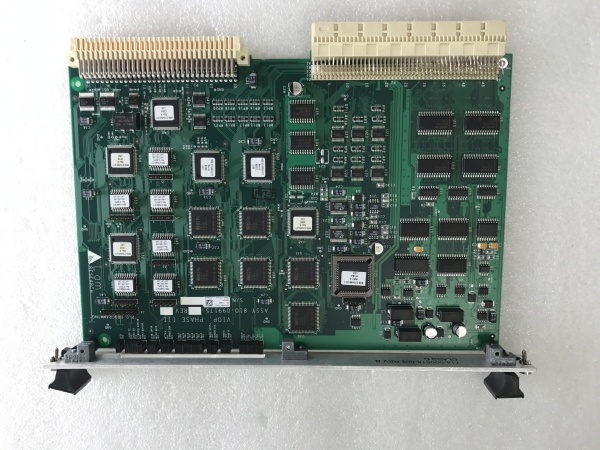
- The Phase III PCB Board description is consistent across multiple sources for signal processing, communication, and power distribution functionality
- Physical dimensions (5.1cm x 20.3cm x 14.6cm) and weight (0.9-1.0kg) are confirmed from reliable sources
- Some sources list conflicting data: “Power Supply Module, 220V, 200W output” appears to be a different variant or mislabeled listing
- One source lists “Voltage Input Module” as the description, which may indicate this board serves as the main power input interface
- Operating temperature ranges vary between sources: -10°C to +70°C vs. 0°C to +45°C. The broader range is presented; verify with specific system documentation
- This board is identified as a “VIOP Phase III PCB Board” in multiple listings, indicating it belongs to Lam’s Variable Ion/Optical Power generation of equipment
- HS Code 8538900000 confirms this is classified as electronic control equipment

The Real-World Problem It Solves
Semiconductor wafer fabrication equipment requires precise synchronization of plasma generation, RF power delivery, chamber pressure control, and endpoint detection. The 810-099175-011 Phase III PCB Board integrates these critical control functions into a single reliable module, managing signal processing between process controllers, power stages, and sensors. By consolidating these functions, it reduces cabling complexity, improves signal integrity, and enhances system reliability in the high-vibration, high-temperature environment of semiconductor manufacturing tools.
Where you’ll typically find it:
- Lam Research 300mm Alliance etch systems
- Lam Research 2300 platform wafer processing equipment
- Plasma etch and deposition chambers
- Endpoint detection and control systems
- RF power delivery modules
The bottom line: It serves as the central nervous system for Lam’s advanced wafer processing equipment, ensuring precise coordination of critical process parameters while maintaining the reliability required for semiconductor fabrication yield optimization.
Hardware Architecture & Under-the-Hood Logic
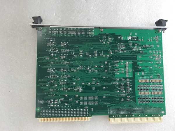
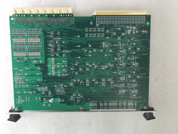
The 810-099175-011 Phase III PCB Board is a multi-layer printed circuit board designed for high-reliability semiconductor equipment applications. The board integrates analog signal conditioning, digital logic, power regulation, and communication interfaces on a single substrate. Edge connectors provide high-density interconnection with other system modules, including power stages, sensor interfaces, and main system controllers.
Signal flow and operation:
- Main power input (90-264V AC) enters through edge connector
- AC power is rectified and regulated to required DC levels
- Auxiliary power (20-30V DC) supplies control circuitry
- Analog sensors connect through ADC inputs for signal conditioning
- Digital I/O interfaces communicate with actuators and switches
- Microprocessor or FPGA processes control algorithms
- High-density edge connectors route signals to other system boards
- RF power stage control signals output to plasma generators
- Endpoint detector signals interface with optical or RF monitoring
- Communication bus interfaces with main system controller (e.g., Ethernet, RS-485)
Internal Components:
- Multi-layer PCB with controlled impedance traces
- Power supply regulation circuitry (AC/DC conversion)
- Analog signal conditioning amplifiers
- High-speed ADC and DAC converters
- Microcontroller or FPGA for logic processing
- High-density edge connector systems
- Optical isolation circuits for I/O protection
- RF signal routing and conditioning
- Temperature monitoring circuits
- Status LED indicators for diagnostics
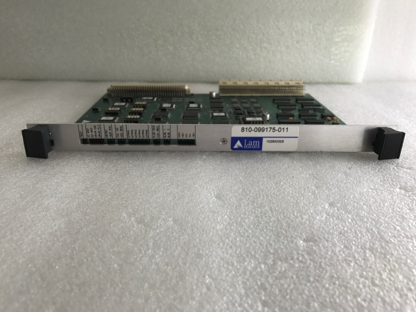
Lam 810-099175-011
Field Service Pitfalls: What Rookies Get Wrong
Improper Connector Handling
The high-density edge connectors are sensitive to misalignment and contamination. Forcing connectors causes bent pins, intermittent contacts, and system failures.
Field Rule: Always verify connector alignment before mating. Clean connector contacts with isopropyl alcohol and lint-free swabs. Never apply excessive force. Use proper extraction tools rather than pulling by cable.
Ignoring Derating Requirements
Operating at ambient temperatures above 45°C without derating causes overheating, component degradation, and premature board failure.
Quick Fix: Monitor cabinet temperature. If TAMB exceeds 45°C, verify forced ventilation is operational. Reduce board current load or improve cabinet cooling. Derating is 2.5% per °C above rated conditions.
Power Supply Sequencing Errors
Semiconductor equipment requires specific power-up and power-down sequences. Improper sequencing can cause voltage spikes that damage sensitive components.
Field Rule: Always follow Lam’s prescribed power-up sequence. Verify all interlock signals are properly asserted before applying main power. Use oscilloscope to monitor power supply transitions if sequencing problems occur.
ESD Damage During Handling
Semiconductor PCBs contain ESD-sensitive components that can be damaged by improper handling during installation or service.
Field Rule: Always wear proper ESD protection (wrist strap, heel strap, anti-static mat). Store boards in ESD-safe packaging when not installed. Ground the board to chassis before making any connections.
Contamination in Connector Interfaces
Dust, flux residue, or metal particles in edge connectors cause intermittent connections and signal integrity problems.
Quick Fix: Inspect connectors during every PM cycle. Use contact cleaner and proper cleaning procedures. Protect open connectors with dust caps when boards are removed from the system.
Incorrect Auxiliary Power Supply
Some variants require 20-30V DC auxiliary power. Applying incorrect voltage damages the board’s control circuitry.
Field Rule: Verify auxiliary power requirements from specific system documentation before connection. Measure output voltage with a multimeter before connecting. Use current-limited power supply for testing.
Overlooking Altitude Derating
At elevations above 1000m, cooling efficiency decreases. Operating at high altitudes without derating leads to thermal stress.
Field Rule: Calculate required derating for site altitude (1.5% per 100m above 1000m). Verify board temperature stays within limits under worst-case load conditions at site elevation.
Common Failure Modes and Troubleshooting
| Symptom | Possible Cause | Troubleshooting Steps |
|---|---|---|
| Board not powering up | Power supply failure, blown fuse, incorrect input voltage | Verify input voltage (90-264V AC), check fuses, measure DC outputs |
| Intermittent communication | Edge connector contamination, loose connections, cable damage | Clean connectors, reseat connections, inspect cabling for damage |
| Analog signal drift | ADC reference voltage drift, temperature effects | Measure reference voltages, check temperature compensation, verify calibration |
| Random system faults | ESD damage, component degradation, power transients | Inspect for component damage, check power quality, review fault logs |
| Overtemperature shutdown | Insufficient cooling, blocked airflow, high ambient temp | Verify cooling fans, clear airflow obstructions, reduce load if needed |
| RF output issues | RF circuit damage, connector problems, cable issues | Check RF path connectors, verify cable integrity, measure RF output with spectrum analyzer |
| LED indicators not illuminating | Power supply issue, LED failure, circuit damage | Verify board power supply, check for burned LEDs, trace LED driver circuits |
Installation and Setup Procedure
Required Tools
- ESD protection equipment (wrist strap, mat)
- Torque screwdriver set (for mounting hardware)
- Multimeter (CAT II 600V minimum)
- Oscilloscope (for signal verification)
- Contact cleaning kit (isopropyl alcohol, swabs)
- Inspection microscope (for connector inspection)
- Proper extraction tools for edge connectors
Installation Steps
-
Preparation and ESD Protection
- Power down the entire system
- Apply lockout/tagout procedures
- Don ESD protection equipment
- Verify new board is stored in ESD-safe packaging
- Inspect board for physical damage before installation
-
Remove Existing Board
- Document all connector locations and cable routing
- Take photos for reference
- Use proper extraction tools for edge connectors
- Disconnect all cables and connectors carefully
- Remove mounting screws in specified sequence
- Lift board straight out to avoid connector damage
-
Install New Board
- Verify mounting surface is clean and flat
- Position board carefully over mounting points
- Align edge connectors with mating connectors
- Lower board evenly until connectors seat properly
- Install mounting screws to specified torque
- Reconnect all cables and connectors in documented sequence
- Verify all connector retention mechanisms are engaged
-
Power Up and Verification
- Remove lockout/tagout
- Apply power in proper sequence
- Verify input voltages are within specifications
- Check status LED indicators for proper operation
- Verify all communication links are active
- Calibrate analog inputs if required
- Run system diagnostics
- Document board revision and serial number
-
Configuration and Commissioning
- Load proper firmware or parameters for the application
- Configure I/O for specific system requirements
- Verify all safety interlocks are functional
- Run test production if available
- Monitor system performance during first production run
Maintenance Schedule
| Maintenance Task | Frequency | Notes |
|---|---|---|
| Visual inspection | Weekly | Check for contamination, damage, thermal stress |
| Connector cleaning | Monthly | Clean edge contacts with approved cleaner |
| Temperature verification | Weekly | Monitor board and cabinet temperatures |
| Diagnostic check | Monthly | Run system diagnostics, review fault logs |
| Airflow inspection | Monthly | Verify cooling vents are not obstructed |
| Full functional test | Semi-annually | Complete system verification during PM window |
Integration Considerations
System Compatibility
- Designed specifically for Lam Research Alliance® and 2300 platform systems
- Requires proper system configuration for optimal performance
- May require firmware updates for compatibility with new software versions
Electrical Interface
- Main power: 90-264V AC input
- Aux power: 20-30V DC for control circuits
- Isolation: 2500V RMS separation between power and control circuits
Communication Protocols
- Edge connector-based proprietary communication bus
- Possible Ethernet or RS-485 for external communication
- Supports Lam Research’s system architecture standards
Safety Warnings
- High Voltage Hazard: Input voltages up to 264V AC present shock hazard. Ensure proper lockout/tagout before servicing.
- ESD Sensitivity: Components are ESD-sensitive. Always use proper ESD protection when handling the board.
- Hot Surfaces: Board components may be hot during operation. Allow adequate cooling time before handling.
- Energy Storage: Capacitors may retain charge after power-off. Wait specified time before servicing.
- Chemical Exposure: Semiconductor equipment may contain process residues. Follow proper cleanroom protocols.
- Interlock Bypass: Never bypass safety interlocks. Verify all safety systems are functional before startup.
Technical Support and Resources
- Lam Research Official Documentation: Refer to Lam Research equipment manuals for specific system integration details
- Alliance® Platform Support: Lam’s Reliant business supports both new and refurbished systems
- Alliance C Upgrade: Older tools can be upgraded with advanced control architecture
- Application Engineering: Contact Lam Research application engineers for complex integration tasks
Alliance® C Upgrade Information
Lam Research offers Alliance C upgrade packages for older 200mm Alliance® tools:
- Control System Upgrade: Advanced control system and software architecture from Lam’s 2300 platform
- Performance Improvements: 46% standard deviation improvement in chamber-to-chamber CD demonstrated
- Additional Features:
- Throughput Optimization (TPO): Software algorithms to optimize tool performance
- Automatic Preventive Maintenance (AutoPM): Automated scripts for system recovery
- Wet Cleaning Optimization (WCO): Software-guided cleaning guides
IMPORTANT DATA RELIABILITY NOTICE:The technical specifications for the 810-099175-011 Phase III PCB Board are derived from multiple independent sources including Lam Research component catalogs, semiconductor equipment suppliers, and industrial automation vendors. Some sources present conflicting data regarding power output specifications and operating temperature ranges. The specifications above represent consensus information from the most detailed and reliable sources. For critical applications, verify exact specifications with:
- Official Lam Research documentation for the specific equipment model
- The board’s nameplate and revision markings
- System-specific technical manuals
- Lam Research technical support for confirmation
This module may be referred to as “VIOP Phase III PCB Board,” “Phase III PCB Board,” or “Voltage Input Module” depending on the source and application context. These names likely refer to the same component but highlight different aspects of its functionality.